- 您现在的位置:买卖IC网 > PDF目录15776 > HA5024EVAL (Intersil)EVALUATION PLATFORM FOR HA5024 PDF资料下载
参数资料
| 型号: | HA5024EVAL |
| 厂商: | Intersil |
| 文件页数: | 14/16页 |
| 文件大小: | 0K |
| 描述: | EVALUATION PLATFORM FOR HA5024 |
| 标准包装: | 1 |
| 主要目的: | 视频,放大器,四路 |
| 嵌入式: | 否 |
| 已用 IC / 零件: | HA5024 |
| 主要属性: | 电流反馈,125MHz,475V/us,±5 V |
| 次要属性: | 7.5mA 静态电流电流,20mA 输出 |
| 已供物品: | 板 |
7
3550.6
February 8, 2006
Application Information
Optimum Feedback Resistor
The plots of inverting and non-inverting frequency response,
see Figure 11 and Figure 12 in the Typical Performance
Curves section, illustrate the performance of the HA5024 in
various closed loop gain configurations. Although the
bandwidth dependency on closed loop gain isn’t as severe
as that of a voltage feedback amplifier, there can be an
appreciable decrease in bandwidth at higher gains. This
decrease may be minimized by taking advantage of the
current feedback amplifier’s unique relationship between
bandwidth and RF. All current feedback amplifiers require a
feedback resistor, even for unity gain applications, and RF,
in conjunction with the internal compensation capacitor, sets
the dominant pole of the frequency response. Thus, the
amplifier’s bandwidth is inversely proportional to RF. The
HA5024 design is optimized for a 1000
R
F at a gain of +1.
Decreasing RF in a unity gain application decreases stability,
resulting in excessive peaking and overshoot. At higher
gains the amplifier is more stable, so RF can be decreased
in a trade-off of stability for bandwidth.
The table below lists recommended RF values for various
gains, and the expected bandwidth.
PC Board Layout
The frequency response of this amplifier depends greatly on
the amount of care taken in designing the PC board. The
use of low inductance components such as chip resistors
and chip capacitors is strongly recommended. If leaded
components are used the leads must be kept short
especially for the power supply decoupling components and
those components connected to the inverting input.
Attention must be given to decoupling the power supplies. A
large value (10
F) tantalum or electrolytic capacitor in
parallel with a small value (0.1
F) chip capacitor works well
in most cases.
A ground plane is strongly recommended to control noise.
Care must also be taken to minimize the capacitance to
ground seen by the amplifier’s inverting input (-IN). The
larger this capacitance, the worse the gain peaking, resulting
in pulse overshoot and possible instability. It is
recommended that the ground plane be removed under
traces connected to -IN, and that connections to -IN be kept
as short as possible to minimize the capacitance from this
node to ground.
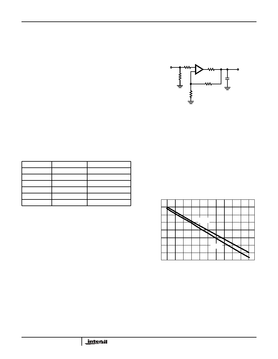
Driving Capacitive Loads
Capacitive loads will degrade the amplifier’s phase margin
resulting in frequency response peaking and possible
oscillations. In most cases the oscillation can be avoided by
placing an isolation resistor (R) in series with the output as
shown in Figure 6.
The selection criteria for the isolation resister is highly
dependent on the load, but 27
has been determined to be
a good starting value.
Power Dissipation Considerations
Due to the high supply current inherent in quad amplifiers, care
must be taken to insure that the maximum junction temperature
(TJ, see Absolute Maximum Ratings) is not exceeded. Figure 7
shows the maximum ambient temperature versus supply
voltage for the available package styles (Plastic DIP, SOIC). At
±5V
DC quiescent operation both package styles may be
operated over the full industrial range of -40°C to 85°C. It is
recommended that thermal calculations, which take into
account output power, be performed by the designer.
Enable/Disable Function
When enabled the amplifier functions as a normal current
feedback amplifier with all of the data in the electrical
specifications table being valid and applicable. When
disabled the amplifier output assumes a true high
impedance state and the supply current is reduced
significantly.
GAIN (ACL)RF ()
BANDWIDTH (MHz)
-1
750
100
+1
1000
125
+2
681
95
+5
1000
52
+10
383
65
-10
750
22
VIN
VOUT
CL
RT
+
-
RI
RF
R
FIGURE 6. PLACEMENT OF THE OUTPUT ISOLATION
RESISTOR, R
100
130
120
110
100
90
70
5
7
9
111315
MAX
.AMBIE
N
T
TEMPE
R
A
T
URE
SUPPLY VOLTAGE (
±V)
PDIP
80
60
50
SOIC
FIGURE 7. MAXIMUM OPERATING AMBIENT TEMPERA-
TURE vs SUPPLY VOLTAGE
HA5024
相关PDF资料 |
PDF描述 |
|---|---|
| CDRH127NP-102MC | POWER INDUCTOR 1.0MH 0.55A SMD |
| MAX6439UTLQVD7+T | IC BATTERY MON SNGL SOT23-6 |
| EL7530EVAL1 | EVALUATION BOARD FOR EL7530 |
| MAX6439UTLQWD3+T | IC BATTERY MON SNGL SOT23-6 |
| MAX6439UTMQWD3+T | IC BATTERY MON SNGL SOT23-6 |
相关代理商/技术参数 |
参数描述 |
|---|---|
| HA5024IB | 功能描述:IC OPAMP QUAD 125MHZ 20-SOIC RoHS:否 类别:集成电路 (IC) >> 线性 - 放大器 - 视频放大器和频缓冲器 系列:- 产品培训模块:Lead (SnPb) Finish for COTS Obsolescence Mitigation Program 标准包装:50 系列:- 应用:TFT-LCD 面板:VCOM 驱动器 输出类型:满摆幅 电路数:1 -3db带宽:35MHz 转换速率:40 V/µs 电流 - 电源:3.7mA 电流 - 输出 / 通道:1.3A 电压 - 电源,单路/双路(±):9 V ~ 20 V,±4.5 V ~ 10 V 安装类型:表面贴装 封装/外壳:8-TSSOP,8-MSOP(0.118",3.00mm 宽)裸露焊盘 供应商设备封装:8-uMax-EP 包装:管件 |
| HA5024IBZ | 功能描述:视频放大器 W/ANL OPAMP4X 125MHZ CFB DISABLE 20W IND RoHS:否 制造商:ON Semiconductor 通道数量:4 电源类型: 工作电源电压:3.3 V, 5 V 电源电流: 最小工作温度: 最大工作温度: 封装 / 箱体:TSSOP-14 封装:Reel |
| HA5024IBZ96 | 功能描述:视频放大器 W/ANL OPAMP4X 125MHZ CFB DISABLE 20W IND RoHS:否 制造商:ON Semiconductor 通道数量:4 电源类型: 工作电源电压:3.3 V, 5 V 电源电流: 最小工作温度: 最大工作温度: 封装 / 箱体:TSSOP-14 封装:Reel |
| HA5024IP | 功能描述:IC AMP VIDEO 125MHZ QUAD 20-PDIP RoHS:否 类别:集成电路 (IC) >> 线性 - 放大器 - 视频放大器和频缓冲器 系列:- 标准包装:1,000 系列:- 应用:驱动器 输出类型:差分 电路数:3 -3db带宽:350MHz 转换速率:1000 V/µs 电流 - 电源:14.5mA 电流 - 输出 / 通道:60mA 电压 - 电源,单路/双路(±):5 V ~ 12 V,±2.5 V ~ 6 V 安装类型:表面贴装 封装/外壳:20-VFQFN 裸露焊盘 供应商设备封装:20-QFN 裸露焊盘(4x4) 包装:带卷 (TR) |
| HA5024IPZ | 功能描述:视频放大器 W/ANNEAL OPAMP 4X 12 5MHZ CFB DISABLE RoHS:否 制造商:ON Semiconductor 通道数量:4 电源类型: 工作电源电压:3.3 V, 5 V 电源电流: 最小工作温度: 最大工作温度: 封装 / 箱体:TSSOP-14 封装:Reel |
发布紧急采购,3分钟左右您将得到回复。