- 您现在的位置:买卖IC网 > PDF目录299169 > HCNW2601-520E 1 CHANNEL LOGIC OUTPUT OPTOCOUPLER, 10 Mbps PDF资料下载
参数资料
| 型号: | HCNW2601-520E |
| 元件分类: | 光电耦合器 |
| 英文描述: | 1 CHANNEL LOGIC OUTPUT OPTOCOUPLER, 10 Mbps |
| 封装: | 0.400 INCH, ROHS COMPLIANT, DIP-8 |
| 文件页数: | 5/21页 |
| 文件大小: | 463K |
| 代理商: | HCNW2601-520E |
13
Notes:
1. Each channel.
2. Peaking circuits may produce transient input currents up to 50 mA, 50 ns maximum pulse width, provided average current does not exceed 20 mA.
3. Peaking circuits may produce transient input currents up to 50 mA, 50 ns maximum pulse width, provided average current does not exceed 15 mA.
4. Derate linearly above 80
°C free-air temperature at a rate of 2.7 mW/°C for the SOIC-8 package.
5. Bypassing of the power supply line is required, with a 0.1
F ceramic disc capacitor adjacent to each optocoupler as illustrated in Figure 17. Total
lead length between both ends of the capacitor and the isolator pins should not exceed 20 mm.
6. The JEDEC registration for the 6N137 specifies a maximum IOH of 250 A. Avago guarantees a maximum IOH of 100 A.
7. The JEDEC registration for the 6N137 specifies a maximum ICCH of 15 mA. Avago guarantees a maximum ICCH of 10 mA.
8. The JEDEC registration for the 6N137 specifies a maximum ICCL of 18 mA. Avago guarantees a maximum ICCL of 13 mA.
9. The JEDEC registration for the 6N137 specifies a maximum IEL of –2.0 mA. Avago guarantees a maximum IEL of -1.6 mA.
10. The tPLH propagation delay is measured from the 3.75 mA point on the falling edge of the input pulse to the 1.5 V point on the rising edge of the
output pulse.
11. The tPHL propagation delay is measured from the 3.75 mA point on the rising edge of the input pulse to the 1.5 V point on the falling edge of the
output pulse.
12. tPSK is equal to the worst case difference in tPHL and/or tPLH that will be seen between units at any given temperature and specified test conditions.
13. See application section titled “Propagation Delay, Pulse-Width Distortion and Propagation Delay Skew” for more information.
14. The tELH enable propagation delay is measured from the 1.5 V point on the falling edge of the enable input pulse to the 1.5 V point on the rising
edge of the output pulse.
15. The tEHL enable propagation delay is measured from the 1.5 V point on the rising edge of the enable input pulse to the 1.5 V point on the falling
edge of the output pulse.
16. CMH is the maximum tolerable rate of rise of the common mode voltage to assure that the output will remain in a high logic state (i.e., VO > 2.0 V).
17. CML is the maximum tolerable rate of fall of the common mode voltage to assure that the output will remain in a low logic state (i.e., VO < 0.8 V).
18. For sinusoidal voltages, (|dVCM | / dt)max = πfCMVCM(p-p).
19. No external pull up is required for a high logic state on the enable input. If the VE pin is not used, tying VE to VCC will result in improved CMR
performance. For single channel products only.
20. Device considered a two-terminal device: pins 1, 2, 3, and 4 shorted together, and pins 5, 6, 7, and 8 shorted together.
21. In accordance with UL1577, each optocoupler is proof tested by applying an insulation test voltage
≥ 4500 V rms for one second (leakage detection
current limit, II-O ≤ 5 A). This test is performed before the 100% production test for partial discharge (Method b) shown in the IEC/EN/DIN EN
60747-5-2 Insulation Characteristics Table, if applicable.
22. In accordance with UL 1577, each optocoupler is proof tested by applying an insulation test voltage
≥ 6000 V rms for one second (leakage detection
current limit, II-O ≤ 5 A). This test is performed before the 100% production test for partial discharge (Method b) shown in the IEC/EN/DIN EN
60747-5-2 Insulation Characteristics Table, if applicable.
23. Measured between the LED anode and cathode shorted together and pins 5 through 8 shorted together. For dual channel products only.
24. Measured between pins 1 and 2 shorted together, and pins 3 and 4 shorted together. For dual channel products only
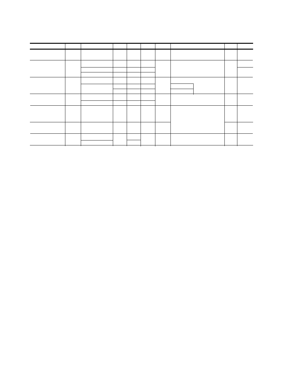
Package Characteristics
All Typicals at TA = 25°C.
Parameter
Sym.
Package
Min.
Typ.
Max.
Units
Test Conditions
Fig.
Note
Input-Output
II-O*
Single 8-Pin DIP
1
A
45% RH, t = 5 s,
20, 21
Insulation
Single SO-8
VI-O = 3 kV dc, TA = 25°C
Input-Output
VISO
8-Pin DIP, SO-8
3750
V rms
RH
≤ 50%, t = 1 min,
20, 21
Momentary With-
Widebody
5000
TA = 25°C
20, 22
stand Voltage**
OPT 020
5000
Input-Output
RI-O
8-Pin DIP, SO-8
1012
VI-O = 500 V dc
1, 20,
Resistance
Widebody
1012
1013
TA = 25°C23
1011
TA = 100°C
Input-Output
CI-O
8-Pin DIP, SO-8
0.6
pF
f = 1 MHz, TA = 25°C
1, 20,
Capacitance
Widebody
0.5
0.6
23
Input-Input
II-I
Dual Channel
0.005
A
RH
≤ 45%, t = 5 s,
24
Insulation
VI-I = 500 V
Leakage Current
Resistance
RI-I
Dual Channel
1011
24
(Input-Input)
Capacitance
CI-I
Dual 8-Pin DIP
0.03
pF
f = 1 MHz
24
(Input-Input)
Dual SO-8
0.25
*JEDEC registered data for the 6N137. The JEDEC Registration specifies 0
°C to 70°C. Avago specifies -40°C to 85°C.
**The Input-Output Momentary Withstand Voltage is a dielectric voltage rating that should not be interpreted as an input-output continuous voltage
rating. For the continuous voltage rating refer to the IEC/EN/DIN EN 60747-5-2 Insulation Characteristics Table (if applicable), your equipment level
safety specification or Avago Application Note 1074 entitled “Optocoupler Input-Output Endurance Voltage.”
For 6N137, HCPL-2601/2611/2630/2631/4661 only.
相关PDF资料 |
PDF描述 |
|---|---|
| HCPL-7800-300 | ISOLATION AMPLIFIER, 3750 V ISOLATION-MIN, 85 kHz BAND WIDTH, PDSO8 |
| HCPL-7800-500 | ISOLATION AMPLIFIER, 3750 V ISOLATION-MIN, 85 kHz BAND WIDTH, PDSO8 |
| HCS273D/SAMPLE | HC/UH SERIES, POSITIVE EDGE TRIGGERED D FLIP-FLOP, TRUE OUTPUT, CDIP20 |
| HCT-21 | 1 ELEMENT, 250 uH, GENERAL PURPOSE INDUCTOR |
| HCT-22 | 1 ELEMENT, 900 uH, GENERAL PURPOSE INDUCTOR |
相关代理商/技术参数 |
参数描述 |
|---|---|
| HCNW2611 | 功能描述:高速光耦合器 10MBd 1Ch 5mA RoHS:否 制造商:Avago Technologies 电流传递比: 最大波特率: 最大正向二极管电压:1.75 V 最大反向二极管电压:5 V 最大功率耗散:40 mW 最大工作温度:+125 C 最小工作温度:- 40 C 封装 / 箱体:SOIC-5 封装:Tube |
| HCNW-2611 | 制造商:Avago Technologies 功能描述:OPTOCOUPLER LOGIC O/P |
| HCNW2611#300 | 功能描述:高速光耦合器 10MBd 1Ch 5mA RoHS:否 制造商:Avago Technologies 电流传递比: 最大波特率: 最大正向二极管电压:1.75 V 最大反向二极管电压:5 V 最大功率耗散:40 mW 最大工作温度:+125 C 最小工作温度:- 40 C 封装 / 箱体:SOIC-5 封装:Tube |
| HCNW-2611#300 | 制造商:Agilent Technologies 功能描述:Logic-gate-output Optocoupler, 1-channel, 5kv Isolation, Dip |
| HCNW2611#500 | 功能描述:高速光耦合器 10MBd 1Ch 5mA RoHS:否 制造商:Avago Technologies 电流传递比: 最大波特率: 最大正向二极管电压:1.75 V 最大反向二极管电压:5 V 最大功率耗散:40 mW 最大工作温度:+125 C 最小工作温度:- 40 C 封装 / 箱体:SOIC-5 封装:Tube |
发布紧急采购,3分钟左右您将得到回复。