- 您现在的位置:买卖IC网 > PDF目录296089 > HCPL-2530-300E (AGILENT TECHNOLOGIES INC) 2 CHANNEL LOGIC OUTPUT OPTOCOUPLER, 1 Mbps PDF资料下载
参数资料
| 型号: | HCPL-2530-300E |
| 厂商: | AGILENT TECHNOLOGIES INC |
| 元件分类: | 光电耦合器 |
| 英文描述: | 2 CHANNEL LOGIC OUTPUT OPTOCOUPLER, 1 Mbps |
| 封装: | 0.300 INCH, LEAD FREE, SURFACE MOUNT, DIP-8 |
| 文件页数: | 3/13页 |
| 文件大小: | 116K |
| 代理商: | HCPL-2530-300E |
11
Notes:
1. Each channel.
2. CURRENT TRANSFER RATIO is defined as
the ratio of output collector current, IO,
to the forward LED input current, IF,
times 100%.
3. Device considered a two-terminal device:
pins 1, 2, 3, and 4 shorted together and
pins 5, 6, 7, and 8 shorted together.
4. Measured between pins 1 and 2 shorted
together, and pins 3 and 4 shorted
together.
5. Common mode transient immunity in a
Logic High level is the maximum tolerable
(positive) dVCM/dt on the rising edge of
the common mode pulse, VCM, to assure
that the output will remain in a Logic High
state (i.e., VO > 2.0 V). Common mode
transient immunity in a Logic Low level is
the maximum tolerable (negative) dVCM/dt
on the falling edge of the common mode
pulse signal, VCM, to assure that the
output will remain in a Logic Low state
(i.e., VO < 0.8 V).
6. The 1.9 k
load represents 1 TTL unit load
of 1.6 mA and the 5.6 k
pull-up resistor.
7. The 4.1 k
load represents 1 LSTTL unit
load of 0.36 mA and the 6.1 k
pull-up
resistor.
8. The frequency at which the ac output
voltage is 3 dB below the low frequency
asymptote.
9. Use of a 0.1
F bypass capacitor
connected between pins 5 and 8 is
recommended.
10. In accordance with UL 1577, each
optocoupler is proof tested by applying an
insulation test voltage
≥4500 V rms for 1
second (leakage detection current limit,
II-O ≤5 A).
11. In accordance with UL 1577, each
optocoupler is proof tested by applying an
insulation test voltage
≥6000 V rms for 1
second (leakage detection current limit,
II-O ≤5 A).
12. Measured between the LED anode and
cathode shorted together and pins 5
through 8 shorted together.
13. Derate linearly above 90
°C free-air
temperature at a rate of 3.0 mW/
°C for
the SOIC-8 package.
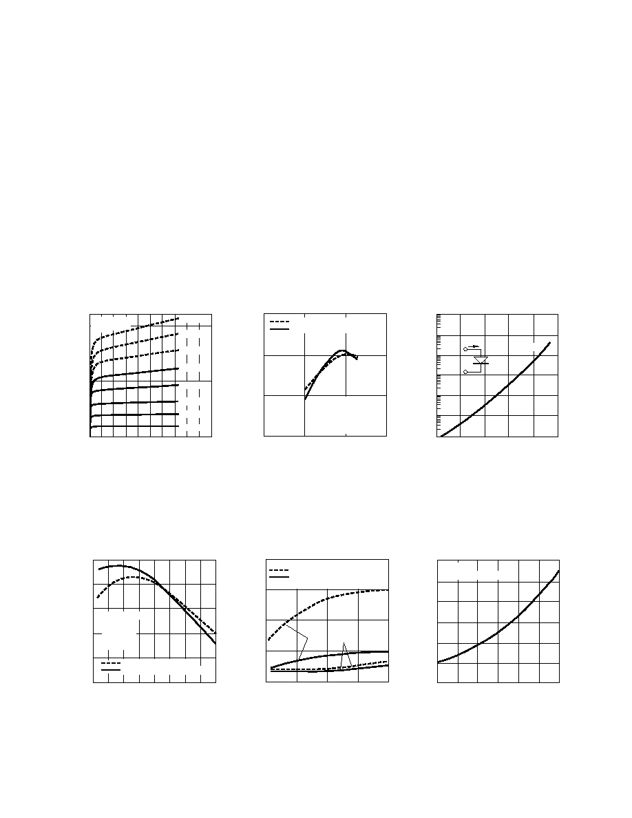
Figure 1. DC and pulsed transfer
characteristics.
Figure 2. Current transfer ratio vs. input
current.
Figure 3. Input current vs. forward voltage.
0
10
20
VO – OUTPUT VOLTAGE – V
I O
–
OUTPUT
CURRENT
–
mA
10
5
0
T = 25°C
V
= 5.0 V
A
CC
40 mA
35 mA
30 mA
25 mA
20 mA
15 mA
10 mA
I = 5 mA
F
NORMALIZED
I = 16 mA
V = 0.5 V
V
= 5 V
T = 25°C
F
O
CC
A
HCPL-2530/0530
HCPL-2531/0531/4534/0534
1.5
1.0
0.5
0.1
0
1
10
100
NORMALIZED
CURRENT
TRANSFER
RATIO
IF – INPUT CURRENT – mA
VF – FORWARD VOLTAGE – VOLTS
100
10
0.1
0.01
1.1
1.2
1.3
1.4
I F
–
FORWARD
CURRENT
–
mA
1.6
1.5
1.0
0.001
1000
IF
VF
+
T = 25°C
A
–
Figure 4. Current transfer ratio vs.
temperature.
Figure 5. Propagation delay vs. temperature.
Figure 6. Logic high output current vs.
temperature.
-50
+50
TA – TEMPERATURE – °C
I
OH
–
LOGIC
HIGH
OUTPUT
CURRENT
–
nA
10-2
-25
0
+25
+75
+100
10 -1
10 0
10+1
10+2
10+3
10+4
VO = VCC = 5.0 V
IF = 0
1.1
1.0
0.9
0.8
0.7
0.6
-60
-20
0
80
NORMALIZED
CURRENT
TRANSFER
RATIO
TA – TEMPERATURE – °C
F
CC
A
-40
20
40
60
100
O
NORMALIZED
I = 16 mA
V = 0.5 V
V
= 5 V
T = 25°C
HCPL-2530/0530
HCPL-2531/0531/4534/0534
2000
1500
1000
500
0
-60
-20
20
60
100
TA – TEMPERATURE – °C
t P
–
PROPAGATION
DELAY
–
ns
tPHL
tPLH
IF = 16 mA, VCC = 5.0 V
HCPL-2530/0530 (RL = 4.1 k)
HCPL-2531/0531/4534/0534
(RL = 1.9 k)
相关PDF资料 |
PDF描述 |
|---|---|
| HCPL-5150 | 0.5 Amp Output Current IGBT Gate Drive Optocoupler |
| HCPL-5150-100 | 0.5 Amp Output Current IGBT Gate Drive Optocoupler |
| HCPL-5150-200 | 0.5 Amp Output Current IGBT Gate Drive Optocoupler |
| HCPL-5150-300 | 0.5 Amp Output Current IGBT Gate Drive Optocoupler |
| HCPL-5151 | 0.5 Amp Output Current IGBT Gate Drive Optocoupler |
相关代理商/技术参数 |
参数描述 |
|---|---|
| HCPL-2530-320E | 功能描述:高速光耦合器 1MBd 2Ch 16mA RoHS:否 制造商:Avago Technologies 电流传递比: 最大波特率: 最大正向二极管电压:1.75 V 最大反向二极管电压:5 V 最大功率耗散:40 mW 最大工作温度:+125 C 最小工作温度:- 40 C 封装 / 箱体:SOIC-5 封装:Tube |
| HCPL-2530-360E | 制造商:AVAGO 制造商全称:AVAGO TECHNOLOGIES LIMITED 功能描述:Dual Channel, High Speed Optocouplers |
| HCPL-2530-500E | 功能描述:高速光耦合器 1MBd 2Ch 16mA RoHS:否 制造商:Avago Technologies 电流传递比: 最大波特率: 最大正向二极管电压:1.75 V 最大反向二极管电压:5 V 最大功率耗散:40 mW 最大工作温度:+125 C 最小工作温度:- 40 C 封装 / 箱体:SOIC-5 封装:Tube |
| HCPL-2530-520E | 功能描述:高速光耦合器 1MBd 2Ch 16mA RoHS:否 制造商:Avago Technologies 电流传递比: 最大波特率: 最大正向二极管电压:1.75 V 最大反向二极管电压:5 V 最大功率耗散:40 mW 最大工作温度:+125 C 最小工作温度:- 40 C 封装 / 箱体:SOIC-5 封装:Tube |
| HCPL-2530-560E | 制造商:AVAGO 制造商全称:AVAGO TECHNOLOGIES LIMITED 功能描述:Dual Channel, High Speed Optocouplers |
发布紧急采购,3分钟左右您将得到回复。