- 您现在的位置:买卖IC网 > PDF目录223876 > HCPL-900J Analog Miscellaneous PDF资料下载
参数资料
| 型号: | HCPL-900J |
| 英文描述: | Analog Miscellaneous |
| 中文描述: | 模拟杂项 |
| 文件页数: | 2/12页 |
| 文件大小: | 264K |
| 代理商: | HCPL-900J |
10
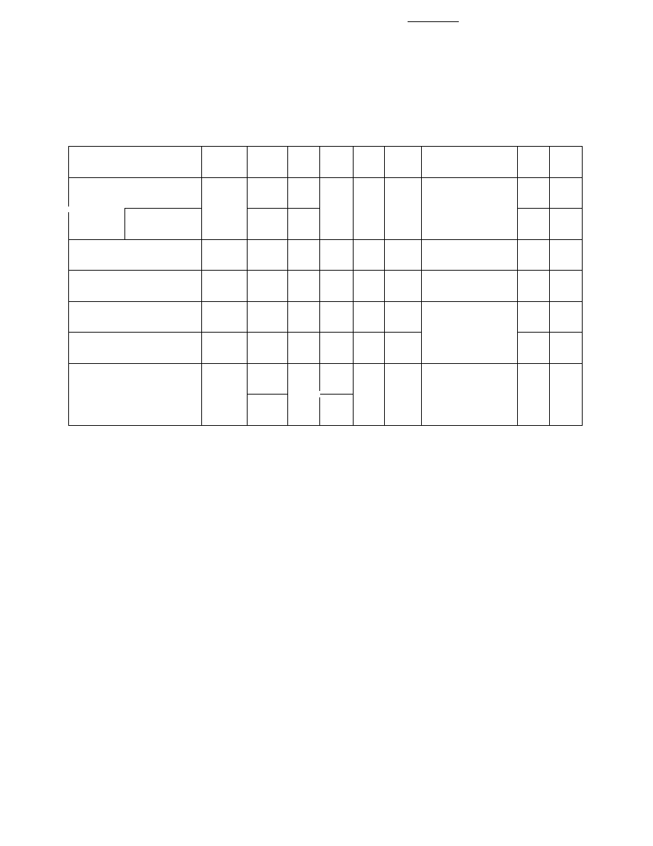
Package Characteristics
Device
Parameter
Symbol HCPL- Min. Typ.* Max. Units
Test Conditions
Fig.
Note
Input-Output Momentary
VISO
2500
V rms
RH
≤ 50%,
4, 9
Withstand Voltage**
t = 1 min.,
Option 020
2730
5000
4, 10
2731
Resistance
RI-O
1012
VI-O = 500 VDC
4
(Input-Output)
RH
≤ 45%
Capacitance
CI-O
0.6
pF
f = 1 MHz
11
(Input-Output)
Input-Input Insulation
II-I
0.005
A
RH
≤ 45%
5
Leakage Current
VI-I = 500 VDC
Input-Input Insulation
RI-I
1011
5
Leakage Current
Capacitance
CI-I
2730
0.03
pF
5
(Input-Input)
2731
0730
0.25
0731
*All Typical values at T
A = 25°C unless otherwise noted.
**The Input-Output Momentary Withstand Voltage is a dielectric voltage rating that should not be interpreted as an input-output
continuous voltage rating. For the continuous voltage rating refer to the VDE 0884 Insulation Characteristics Table (if appli-
cable), your equipment level safety specification or Agilent Application Note 1074 entitled “Optocoupler Input-Output Endurance
Voltage.”
Notes:
1. Pin 5 should be the most negative
voltage at the detector side.
2. Each channel.
3. DC CURRENT TRANSFER RATIO
(CTR) is defined as the ratio of output
collector current, I
O, to the forward
LED input current, I
F, times 100%.
4. Device considered a two-terminal
device: pins 1, 2, 3, and 4 shorted
together, and pins 5, 6, 7, and 8
shorted together.
5. Measured between pins 1 and 2
shorted together, and pins 3 and 4
shorted together.
6. Common mode transient immunity in a
Logic High level is the maximum
tolerable (positive) dV
CM/dt of the
TA = 25°C
common mode pulse, V
CM, to assure
that the output will remain in a Logic
High state (i.e., V
O > 2.0 V). Common
mode transient immunity in a Logic
Low level is the maximum tolerable
(negative) dV
CM/dt of the common
mode pulse, V
CM, to assure that the
output will remain in a Logic Low state
(i.e., V
O < 0.8 V).
7. In applications where dV/dt may
exceed 50,000 V/
s (such as static
discharge) a series resistor, R
CC,
should be included to protect the
detector IC from destructively high
surge currents. The recommended
value is R
CC = 110 .
8. Use of a 0.1
F bypass capacitor
connected between pins 5 and 8
adjacent to the device is
recommended.
9. In accordance with UL 1577, each
optocoupler is proof tested by
applying an insulation test voltage
> 3000 V rms for 1 second (leakage
detection current limit, I
I-O < 5 A).
10. In accordance with UL 1577, each
optocoupler is proof tested by
applying an insulation test voltage
> 6000 V rms for 1 second (leakage
detection current limit, I
I-O < 5 A).
11. Measured between the LED anode and
cathode shorted together and pins 5
through 8 shorted together.
12. Derate linearly above 65
°C free-air
temperature at a rate of 2.3 mW/
°C for
the SO-8 package.
相关PDF资料 |
PDF描述 |
|---|---|
| HCPL-900J-500 | Analog Miscellaneous |
| HCPL-901J | Analog Miscellaneous |
| HCPL-901J-500 | Analog Miscellaneous |
| HCPL-902J | Analog Miscellaneous |
| HCPL-902J-500 | Analog Miscellaneous |
相关代理商/技术参数 |
参数描述 |
|---|---|
| HCPL-900J-000E | 功能描述:隔离器接口集成电路 Digital Isolator (100MBd) RoHS:否 制造商:Texas Instruments 通道数量:2 传播延迟时间: 电源电压-最大:5.5 V 电源电压-最小:3 V 电源电流:3.6 mA 功率耗散: 最大工作温度:+ 125 C 安装风格: 封装 / 箱体:SOIC-8 封装:Tube |
| HCPL-900J-500 | 功能描述:隔离放大器 Digital Isolator (100MBd) RoHS:否 制造商:Texas Instruments 输入补偿电压:1.5 mV 共模抑制比(最小值):95 dB 带宽:60 KHz 工作电源电压:3.3 V 电源电流:8 mA 工作温度范围:- 40 C to + 105 C 安装风格:SMD/SMT 封装 / 箱体:SOP-8 封装:Tube |
| HCPL-900J-500E | 功能描述:隔离放大器 Digital Isolator (100MBd) RoHS:否 制造商:Texas Instruments 输入补偿电压:1.5 mV 共模抑制比(最小值):95 dB 带宽:60 KHz 工作电源电压:3.3 V 电源电流:8 mA 工作温度范围:- 40 C to + 105 C 安装风格:SMD/SMT 封装 / 箱体:SOP-8 封装:Tube |
| HCPL-901J | 功能描述:隔离放大器 Digital Isolator (100MBd) RoHS:否 制造商:Texas Instruments 输入补偿电压:1.5 mV 共模抑制比(最小值):95 dB 带宽:60 KHz 工作电源电压:3.3 V 电源电流:8 mA 工作温度范围:- 40 C to + 105 C 安装风格:SMD/SMT 封装 / 箱体:SOP-8 封装:Tube |
| HCPL-901J-000E | 功能描述:隔离放大器 Digital Isolator (100MBd) RoHS:否 制造商:Texas Instruments 输入补偿电压:1.5 mV 共模抑制比(最小值):95 dB 带宽:60 KHz 工作电源电压:3.3 V 电源电流:8 mA 工作温度范围:- 40 C to + 105 C 安装风格:SMD/SMT 封装 / 箱体:SOP-8 封装:Tube |
发布紧急采购,3分钟左右您将得到回复。