- 您现在的位置:买卖IC网 > PDF目录385375 > HFA1110 (Intersil Corporation) 750MHz, Low Distortion Unity Gain,Closed Loop Buffer(750MHz,低失真单位增益,闭环缓冲器) PDF资料下载
参数资料
| 型号: | HFA1110 |
| 厂商: | Intersil Corporation |
| 英文描述: | 750MHz, Low Distortion Unity Gain,Closed Loop Buffer(750MHz,低失真单位增益,闭环缓冲器) |
| 中文描述: | 750MHz的低失真单位增益,闭环缓冲器(750MHz的低失真单位增益,闭环缓冲器) |
| 文件页数: | 3/9页 |
| 文件大小: | 184K |
| 代理商: | HFA1110 |
3
FN2944.8
June 6, 2006
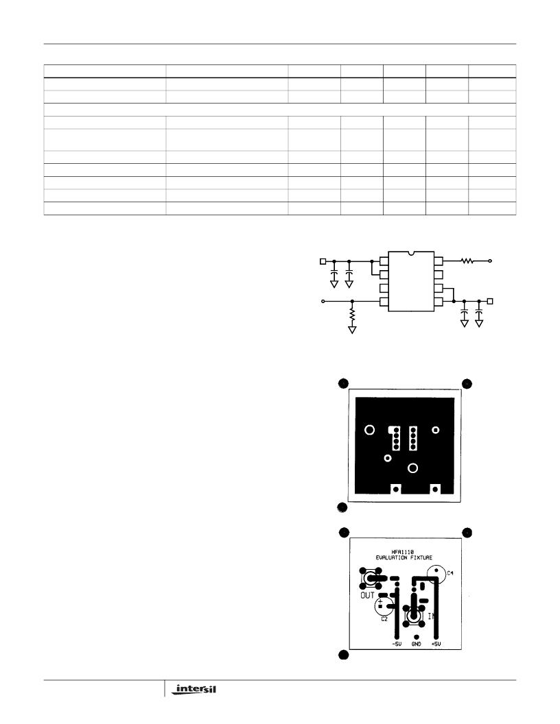
Application Information
PC Board Layout
The frequency performance of this amplifier depends a great
deal on the amount of care taken in designing the PC board.
The use of low inductance components such as chip
resistors and chip capacitors is strongly recommended,
while a solid ground plane is a must!
Attention should be given to decoupling the power supplies.
A large value (10
μ
F) tantalum in parallel with a small value
chip (0.1
μ
F) capacitor works well in most cases.
Terminated microstrip signal lines are recommended at the
input and output of the device. Output capacitance, such as
that resulting from an improperly terminated transmission
line will degrade the frequency response of the amplifier and
may cause oscillations. In most cases, the oscillation can be
avoided by placing a resistor (R
S
) in series with the output.
See the “Recommended R
S
vs Load Capacitance” graph for
specific recommendations.
An example of a good high frequency layout is the
Evaluation Board shown below.
Evaluation Board
An evaluation board is available for the HFA1110 (part
number HFA1110EVAL). Please contact your local sales
office for information.
The layout and schematic of the board are shown here:
NOTE: The SOIC version may be evaluated in the DIP board by
using a SOIC-to-DIP adapter such as Aries Electronics Part Number
08-350000-10.
-1dB Gain Compression
100MHz
25
-
14
-
dBm
Reverse Gain (S
12
, Note 2)
TRANSIENT RESPONSE
100MHz, V
OUT
= 1V
P-P
25
-
-60
-
dB
Rise Time
V
OUT
= 0.5V Step
V
OUT
= 1.0V Step, Input Signal
Rise/Fall = 1ns
25
-
0.5
-
ns
Overshoot (Note 2)
25
-
2.5
-
%
0.2% Settling Time (Note 2)
V
OUT
= 1V to 0V
V
OUT
= 1V to 0V
25
-
7
-
ns
0.1% Settling Time (Note 2)
25
-
11
-
ns
Overdrive Recovery Time
25
-
15
-
ns
Differential Gain
3.58MHz, R
L
= 75
3.58MHz, R
L
= 75
25
-
0.04
-
%
Differential Phase
25
-
0.025
-
°
NOTE:
2. See Typical Performance Curves for more information.
Electrical Specifications
V
SUPPLY
=
±
5V, R
L
= 100
, Unless Otherwise Specified
(Continued)
TEST CONDITIONS
PARAMETER
TEMP (°C)
MIN
TYP
MAX
UNITS
50
1
2
3
4
8
7
6
5
+5V
0.1
μ
F
10
μ
F
50
OUT
0.1
μ
F
10
μ
F
-5V
HFA1110
IN
R
S
SCHEMATIC DIAGRAM
BOTTOM LAYOUT
TOP LAYOUT
1
HFA1110
相关PDF资料 |
PDF描述 |
|---|---|
| HFA1112 | Ultra High Speed Programmable Gain Buffer Amplifier(超高速可编程增益缓冲器放大器) |
| HFA1113 | 850MHz, Low Distortion, Output Limiting, Programmable Gain, Buffer Amplifier(850MHz、低失真、输出限定可编程增益缓冲放大器) |
| HFA1115883 | High Speed, Low Power, Output Limiting Closed Loop Buffer Amplifier |
| HFA1115IP | Mini-Stripax Plus Replacement Blade; Conductor Size AWG:24-22; Features:Includes top & bottom blades, spring & wire stop; Specially formed stripping blades ensure no damage to the conductor; Easy to install RoHS Compliant: Yes |
| HFA1115IB | SINGLEMODE FIBER PATCH CABLE, PLENUM SC-LC 10M |
相关代理商/技术参数 |
参数描述 |
|---|---|
| HFA1110/883 | 制造商:INTERSIL 制造商全称:Intersil Corporation 功能描述:750MHz, Low Distortion 750MHz, Low Distortion |
| HFA1110_06 | 制造商:INTERSIL 制造商全称:Intersil Corporation 功能描述:750MHz, Low Distortion Unity Gain, Closed Loop Buffer |
| HFA1110883 | 制造商:INTERSIL 制造商全称:Intersil Corporation 功能描述:750MHz, Low Distortion 750MHz, Low Distortion |
| HFA1110EVAL | 功能描述:EVALUATION PLATFORM HFA1110 RoHS:否 类别:编程器,开发系统 >> 评估板 - 运算放大器 系列:- 产品培训模块:Lead (SnPb) Finish for COTS Obsolescence Mitigation Program 标准包装:1 系列:- |
| HFA1110IB | 功能描述:IC BUFFER CFA 750MHZ 8-SOIC RoHS:否 类别:集成电路 (IC) >> Linear - Amplifiers - Instrumentation 系列:- 标准包装:50 系列:LinCMOS™ 放大器类型:通用 电路数:4 输出类型:- 转换速率:0.05 V/µs 增益带宽积:110kHz -3db带宽:- 电流 - 输入偏压:0.7pA 电压 - 输入偏移:210µV 电流 - 电源:57µA 电流 - 输出 / 通道:30mA 电压 - 电源,单路/双路(±):3 V ~ 16 V,±1.5 V ~ 8 V 工作温度:-40°C ~ 85°C 安装类型:表面贴装 封装/外壳:14-SOIC(0.154",3.90mm 宽) 供应商设备封装:14-SOIC 包装:管件 产品目录页面:865 (CN2011-ZH PDF) 其它名称:296-1834296-1834-5 |
发布紧急采购,3分钟左右您将得到回复。