- 您现在的位置:买卖IC网 > PDF目录385375 > HFA1112 (Intersil Corporation) Ultra High Speed Programmable Gain Buffer Amplifier(超高速可编程增益缓冲器放大器) PDF资料下载
参数资料
| 型号: | HFA1112 |
| 厂商: | Intersil Corporation |
| 英文描述: | Ultra High Speed Programmable Gain Buffer Amplifier(超高速可编程增益缓冲器放大器) |
| 中文描述: | 超高速可编程增益缓冲放大器(超高速可编程增益缓冲器放大器) |
| 文件页数: | 4/14页 |
| 文件大小: | 482K |
| 代理商: | HFA1112 |
4
Application Information
Closed Loop Gain Selection
The HFA1112 features a novel design which allows the user
to select from three closed loop gains, without any external
components. The result is a more flexible product, fewer part
types in inventory, and more efficient use of board space.
This “buffer” operates in closed loop gains of -1, +1, or +2, and
gain selection is accomplished via connections to the
±
inputs.
Applying the input signal to +IN and floating -IN selects a gain
of +1, while grounding -IN selects a gain of +2. A gain of -1 is
obtained by applying the input signal to -IN with +IN grounded.
The table below summarizes these connections:
PC Board Layout
The frequency response of this amplifier depends greatly on
the amount of care taken in designing the PC board.
The
use of low inductance components such as chip
resistors and chip capacitors is strongly recommended,
while a solid ground plane is a must!
Attention should be given to decoupling the power supplies.
A large value (10
μ
F) tantalum in parallel with a small value
(0.1
μ
F) chip capacitor works well in most cases.
Terminated microstrip signal lines are recommended at the
input and output of the device. Capacitance directly on the
output must be minimized, or isolated as discussed in the
next section.
For unity gain applications, care must also be taken to
minimize the capacitance to ground seen by the amplifier’s
inverting input. At higher frequencies this capacitance will
tend to short the -INPUT to GND, resulting in a closed loop
gain which increases with frequency. This will cause
excessive high frequency peaking and potentially other
problems as well.
An example of a good high frequency layout is the
Evaluation Board shown in Figure 2.
Driving Capacitive Loads
Capacitive loads, such as an A/D input, or an improperly
terminated transmission line will degrade the amplifier’s
phase margin resulting in frequency response peaking and
possible oscillations. In most cases, the oscillation can be
avoided by placing a resistor (R
S
) in series with the output
prior to the capacitance.
Figure 1 details starting points for the selection of this
resistor. The points on the curve indicate the R
S
and C
L
combinations for the optimum bandwidth, stability, and
settling time, but experimental fine tuning is recommended.
Picking a point above or to the right of the curve yields an
overdamped response, while points below or left of the curve
indicate areas of underdamped performance.
R
S
and C
L
form a low pass network at the output, thus
limiting system bandwidth well below the amplifier
bandwidth of 850MHz. By decreasing R
S
as C
L
increases
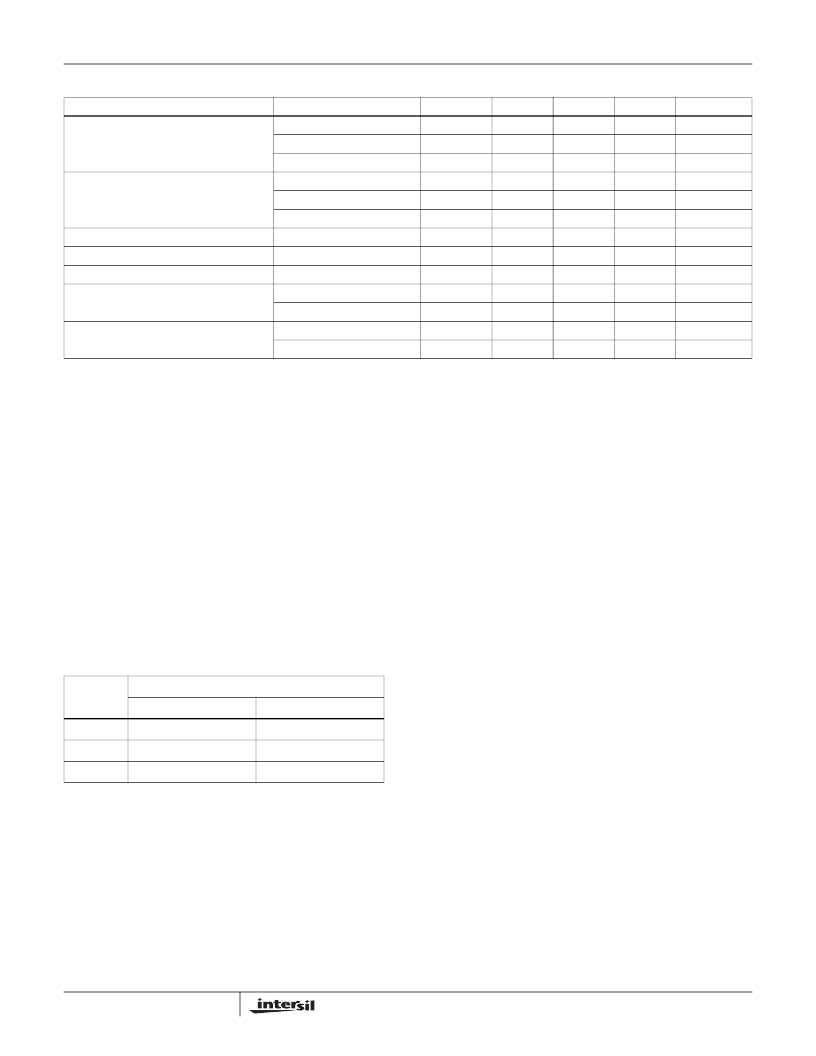
Rise Time
(V
OUT
= 2V Step)
A
V
= -1
A
V
= +1
A
V
= +2
A
V
= -1
A
V
= +1
A
V
= +2
V
OUT
= 2V to 0V
V
OUT
= 2V to 0V
V
IN
= 5V
P-P
A
V
= +1, 3.58MHz, R
L
= 150
A
V
= +2, 3.58MHz, R
L
= 150
A
V
= +1, 3.58MHz, R
L
= 150
A
V
= +2, 3.58MHz, R
L
= 150
25
-
0.82
-
ns
25
-
1.06
-
ns
25
-
1.00
-
ns
Overshoot
(V
OUT
= 0.5V Step, Input t
R
/t
F
= 200ps,
Notes 2, 3, 4)
25
-
12
30
%
25
-
45
65
%
25
-
6
20
%
0.1% Settling Time (Note 3)
25
-
11
-
ns
0.05% Settling Time
25
-
15
-
ns
Overdrive Recovery Time
25
-
8.5
-
ns
Differential Gain
25
-
0.03
-
%
25
-
0.02
-
%
Differential Phase
25
-
0.05
-
Degrees
25
-
0.04
-
Degrees
NOTES:
2. This parameter is not tested. The limits are guaranteed based on lab characterization, and reflect lot-to-lot variation.
3. See Typical Performance Curves for more information.
4. Overshoot decreases as input transition times increase, especially for A
V
= +1. Please refer to Typical Performance Curves.
Electrical Specifications
V
SUPPLY
=
±
5V, A
V
= +1, R
L
= 100
, Unless Otherwise Specified
(Continued)
PARAMETER
TEST CONDITIONS
TEMP (
o
C)
MIN
TYP
MAX
UNITS
GAIN
(A
CL
)
CONNECTIONS
+INPUT (PIN 3)
-INPUT (PIN 2)
-1
GND
Input
+1
Input
NC (Floating)
+2
Input
GND
HFA1112
相关PDF资料 |
PDF描述 |
|---|---|
| HFA1113 | 850MHz, Low Distortion, Output Limiting, Programmable Gain, Buffer Amplifier(850MHz、低失真、输出限定可编程增益缓冲放大器) |
| HFA1115883 | High Speed, Low Power, Output Limiting Closed Loop Buffer Amplifier |
| HFA1115IP | Mini-Stripax Plus Replacement Blade; Conductor Size AWG:24-22; Features:Includes top & bottom blades, spring & wire stop; Specially formed stripping blades ensure no damage to the conductor; Easy to install RoHS Compliant: Yes |
| HFA1115IB | SINGLEMODE FIBER PATCH CABLE, PLENUM SC-LC 10M |
| HFA1115EVAL | 225MHz, Low Power, Output Limiting, Closed Loop Buffer Amplifier |
相关代理商/技术参数 |
参数描述 |
|---|---|
| HFA1112 WAF | 制造商:Intersil Corporation 功能描述: |
| HFA1112/883 | 制造商:INTERSIL 制造商全称:Intersil Corporation 功能描述:Ultra High Speed Programmable Gain Buffer Amplifier |
| HFA1112_05 | 制造商:INTERSIL 制造商全称:Intersil Corporation 功能描述:850MHz, Low Distortion Programmable Gain Buffer Amplifiers |
| HFA1112883 | 制造商:INTERSIL 制造商全称:Intersil Corporation 功能描述:Ultra High Speed Programmable Gain Buffer Amplifier |
| HFA1112A | 制造商:INTERSIL 制造商全称:Intersil Corporation 功能描述:850MHz, Low Distortion Programmable Gain Buffer Amplifiers |
发布紧急采购,3分钟左右您将得到回复。