- 您现在的位置:买卖IC网 > PDF目录385375 > HFA1135IB96 (INTERSIL CORP) GT 3C 3#16S SKT RECP BOX PDF资料下载
参数资料
| 型号: | HFA1135IB96 |
| 厂商: | INTERSIL CORP |
| 元件分类: | 音频/视频放大 |
| 英文描述: | GT 3C 3#16S SKT RECP BOX |
| 中文描述: | 1 CHANNEL, VIDEO PREAMPLIFIER, PDSO8 |
| 封装: | PLASTIC, MS-012AA, SOIC-8 |
| 文件页数: | 5/15页 |
| 文件大小: | 220K |
| 代理商: | HFA1135IB96 |
5
problems due to the feedback impedance decrease at higher
frequencies). At higher gains the amplifier is more stable, so
R
F
can be decreased in a trade-off of stability for bandwidth.
The table below lists recommended R
F
values, and the
expected bandwidth, for various closed loop gains.
Non-inverting Input Source Impedance
For best operation, the DC source impedance seen by the
non-inverting input should be
≥
50
.
This is especially
important in inverting gain configurations where the non-
inverting input would normally be connected directly to GND.
Pulse Undershoot and Asymmetrical Slew Rates
The HFA1135 utilizes a quasi-complementary output stage
to achieve high output current while minimizing quiescent
supply current. In this approach, a composite device
replaces the traditional PNP pulldown transistor. The
composite device switches modes after crossing 0V,
resulting in added distortion for signals swinging below
ground, and an increased undershoot on the negative
portion of the output waveform (see Figures 9, 13, and 17).
This undershoot isn’t present for small bipolar signals, or
large positive signals. Another artifact of the composite
device is asymmetrical slew rates for output signals with a
negative voltage component. The slew rate degrades as the
output signal crosses through 0V (see Figures 9, 13, and
17), resulting in a slower overall negative slew rate. Positive
only signals have symmetrical slew rates as illustrated in the
large signal positive pulse response graphs (see Figures 7,
11, and 15).
PC Board Layout
This amplifier’s frequency response depends greatly on the
care taken in designing the PC board.
The use of low
inductance components such as chip resistors and chip
capacitors is strongly recommended, while a solid
ground plane is a must!
Attention should be given to decoupling the power supplies.
A large value (10
μ
F) tantalum in parallel with a small value
(0.1
μ
F) chip capacitor works well in most cases.
Terminated microstrip signal lines are recommended at the
input and output of the device. Capacitance directly on the
output must be minimized, or isolated as discussed in the
next section.
Care must also be taken to minimize the capacitance to
ground at the amplifier’s inverting input (-IN), as this
capacitance causes gain peaking, pulse overshoot, and if
large enough, instability. To reduce this capacitance, the
designer should remove the ground plane under traces
connected to -IN, and keep connections to -IN as short as
possible.
An example of a good high frequency layout is the
Evaluation Board shown in Figure 2.
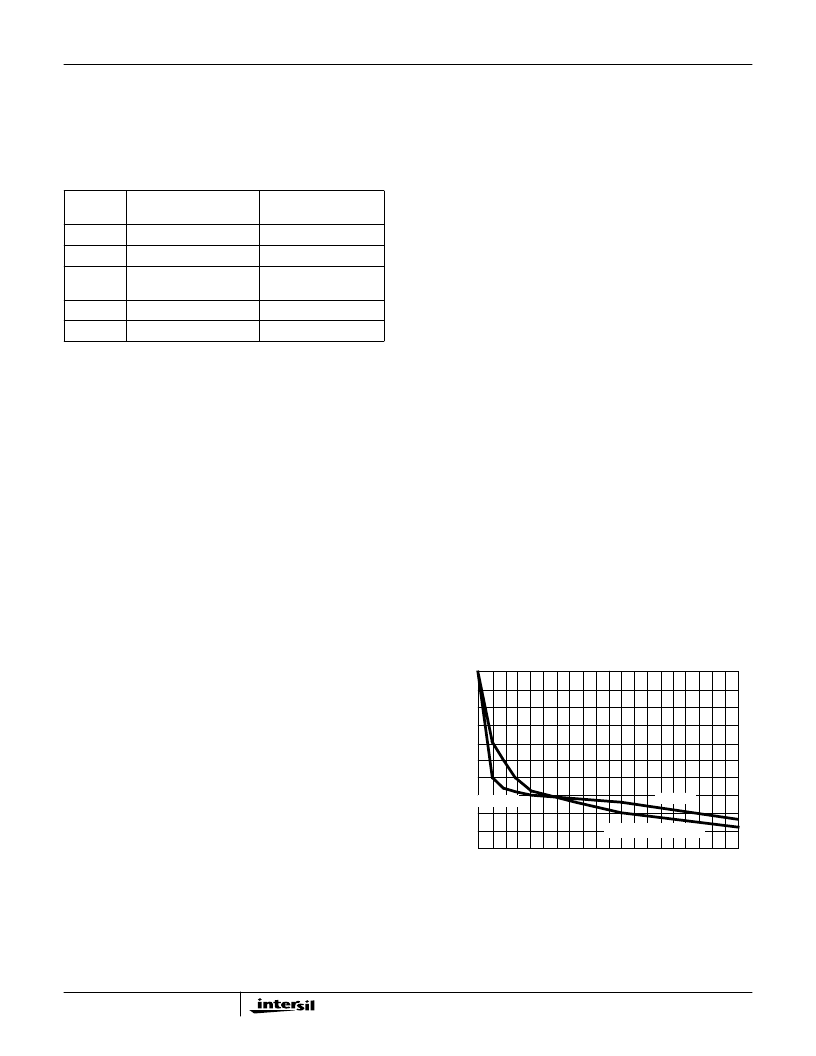
Driving Capacitive Loads
Capacitive loads, such as an A/D input, or an improperly
terminated transmission line degrade the amplifier’s phase
margin resulting in frequency response peaking and
possible oscillations. In most cases, the oscillation can be
avoided by placing a resistor (R
S
) in series with the output
prior to the capacitance.
Figure 1 details starting points for the selection of this
resistor. The points on the curve indicate the R
S
and C
L
combinations for the optimum bandwidth, stability, and
settling time, but experimental fine tuning is recommended.
Picking a point above or to the right of the curve yields an
overdamped response, while points below or left of the curve
indicate areas of underdamped performance.
R
S
and C
L
form a low pass network at the output, thus
limiting system bandwidth well below the amplifier bandwidth
of 660MHz (A
V
= +1). By decreasing R
S
as C
L
increases (as
illustrated by the curves), the maximum bandwidth is
obtained without sacrificing stability. In spite of this,
bandwidth still decreases as the load capacitance increases.
For example, at A
V
= +1, R
S
= 50
, C
L
= 20pF, the overall
bandwidth is 170MHz, but the bandwidth drops to 45MHz at
A
V
= +1, R
S
= 10
, C
L
= 330pF.
TABLE 1. OPTIMUM FEEDBACK RESISTOR
GAIN
(A
V
)
R
F
(
)
BANDWIDTH
(MHz)
-1
330
290
+1
1.5k
660
+2
250
330
360
315
+5
180
200
+10
250
90
R
S
)
LOAD CAPACITANCE (pF)
50
45
40
35
30
25
20
15
10
5
0
0
40
80
120
160
200
240
280
320
360
400
A
V
= +1
A
V
= +2, R
F
= 250
FIGURE 1. RECOMMENDED SERIES RESISTOR vs LOAD
CAPACITANCE
A
V
= +1
HFA1135
相关PDF资料 |
PDF描述 |
|---|---|
| HFA1135IB | 360MHz, Low Power, Video Operational Amplifier with Output Limiting |
| HFA1135EVAL | 360MHz, Low Power, Video Operational Amplifier with Output Limiting |
| HFA1135 | 360MHz, Low Power, Video Operational Amplifier with Output Limiting(360MHz、低功耗视频运算放大器(带输出限制)) |
| HFA1205IP | 2.5V 144-mc CPLD - NOT RECOMMENDED for NEW DESIGN |
| HFA1205IB | Circular Connector; MIL SPEC:MIL-C-26482, Series I, Solder; Body Material:Aluminum; Series:PT06; No. of Contacts:55; Connector Shell Size:22; Connecting Termination:Solder; Circular Shell Style:Straight Plug |
相关代理商/技术参数 |
参数描述 |
|---|---|
| HFA1135IBZ | 功能描述:视频放大器 W/ANNEAL OPAMP 360MH ZCFBLIMIT8SOICIND RoHS:否 制造商:ON Semiconductor 通道数量:4 电源类型: 工作电源电压:3.3 V, 5 V 电源电流: 最小工作温度: 最大工作温度: 封装 / 箱体:TSSOP-14 封装:Reel |
| HFA1135IBZ | 制造商:Intersil Corporation 功能描述:IC VIDEO OP AMP 360MHZ |
| HFA1135IBZ96 | 功能描述:视频放大器 W/ANNEAL OPAMP 360MHZ CFB LIMIT IND RoHS:否 制造商:ON Semiconductor 通道数量:4 电源类型: 工作电源电压:3.3 V, 5 V 电源电流: 最小工作温度: 最大工作温度: 封装 / 箱体:TSSOP-14 封装:Reel |
| HFA1135MJ/883 | 制造商:Rochester Electronics LLC 功能描述:- Bulk |
| HFA1135ML/883 | 制造商:Rochester Electronics LLC 功能描述:- Bulk |
发布紧急采购,3分钟左右您将得到回复。