- 您现在的位置:买卖IC网 > PDF目录385375 > HFA1135IB (INTERSIL CORP) 360MHz, Low Power, Video Operational Amplifier with Output Limiting PDF资料下载
参数资料
| 型号: | HFA1135IB |
| 厂商: | INTERSIL CORP |
| 元件分类: | 音频/视频放大 |
| 英文描述: | 360MHz, Low Power, Video Operational Amplifier with Output Limiting |
| 中文描述: | 1 CHANNEL, VIDEO PREAMPLIFIER, PDSO8 |
| 封装: | PLASTIC, MS-012AA, SOIC-8 |
| 文件页数: | 7/15页 |
| 文件大小: | 220K |
| 代理商: | HFA1135IB |
7
When the output is limited, the negative input continues to
source a slewing current (I
LIMIT
) in an attempt to force the
output to the quiescent voltage defined by the input. Q
P5
must sink this current while limiting, because the -IN current
is always mirrored onto the high impedance node. The
limiting current is calculated as:
I
LIMIT
= (V
-IN
- V
OUT LIMITED
)/R
F
+ V
-IN
/R
G
.
As an example, a unity gain circuit with V
IN
= 2V, and V
H
= 1V,
would have I
LIMIT
= (2V - 1V)/1.5k
+ 2V/
∞
= 667
μ
A (R
G
=
∞
for unity gain applications). Note that I
CC
increases by I
LIMIT
when the output is limited.
Limit Accuracy
The limited output voltage will not be exactly equal to the
voltage applied to V
H
or V
L
. Offset errors, mostly due to VBE
mismatches, necessitate a limit accuracy parameter which is
found in the device specifications. Limit accuracy is a
function of the limiting conditions. Referring again to Figure
3, it can be seen that one component of limit accuracy is the
V
BE
mismatch between the Q
X6
transistors, and the Q
X5
transistors. If the transistors always ran at the same current
level there would be no V
BE
mismatch, and no contribution
to the inaccuracy. The Q
X6
transistors are biased at a
constant current, but as described earlier, the current
through Q
X5
is equivalent to I
LIMIT
. V
BE
increases as I
LIMIT
increases, causing the limited output voltage to increase as
well. I
LIMIT
is a function of the overdrive level
((A
V
x V
IN
- V
LIMIT
) / V
LIMIT
), so limit accuracy degrades as
the overdrive increases. For example, accuracy degrades
from +15mV to +70mV when the overdrive increases from
100% to 200% (A
V
= +2, V
H
= 500mV, R
F
= 250
).
Consideration must also be given to the fact that the limit
voltages have an effect on amplifier linearity. The “Linearity
Near Limit Voltage” curves, Figures 34 and 35, illustrate the
impact of several limit levels on linearity.
Limit Range
Unlike some competitor devices, both V
H
and V
L
have usable
ranges that cross 0V. While V
H
must be more positive than
V
L
, both may be positive or negative, within the range
restrictions indicated in the specifications. For example, the
HFA1135 could be limited to ECL output levels by setting
V
H
= -0.8V and V
L
= -1.8V. V
H
and V
L
may be connected to
the same voltage (GND for instance) but the result won’t be a
DC output voltage from an AC input signal. A 150mV - 200mV
AC signal will still be present at the output.
Recovery from Overdrive
The output voltage remains at the limit level as long as the
overdrive condition remains. When the input voltage drops
below the overdrive level (V
LIMIT
/A
V
) the amplifier returns to
linear operation. A time delay, known as the Overdrive
Recovery Time, is required for this resumption of linear
operation. Overdrive recovery time is defined as the
difference between the amplifier’s propagation delay exiting
limiting and the amplifier’s normal propagation delay, and it is
a strong function of the overdrive level. Figure 36 details the
overdrive recovery time for various limit and overdrive levels.
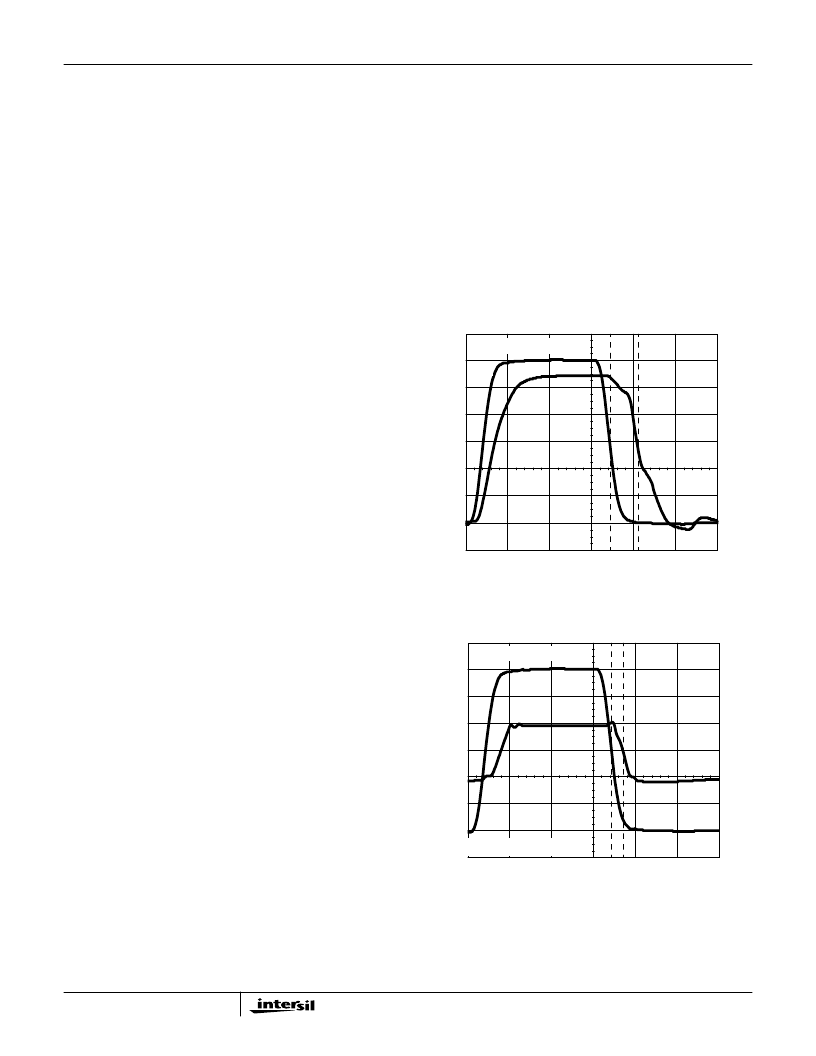
Benefits of Output Limiting
The plots of “Pulse Response Without Limiting” and “Pulse
Response With Limiting” (Figures 4 and 5) highlight the
advantages of output limiting. Besides the obvious benefit of
constraining the output swing to a defined range, limiting the
output excursions also keeps the output transistors from
saturating, which prevents unwanted saturation artifacts
from distorting the output signal. Output limiting also takes
advantage of the HFA1135’s ultra-fast overdrive recovery
time, reducing the recovery time from 2.3ns to 0.3ns, based
on the amplifier’s normal propagation delay of 1.2ns.
FIGURE 4. PULSE RESPONSE WITHOUT LIMITING
FIGURE 5. PULSE RESPONSE WITH LIMITING
TIME (5ns/DIV.)
I
A
V
= +2, R
F
= 250
0
OUT
-0.5
-1.0
0.5
1.0
1.5
2.0
O
0
-1.0
-2.0
1.0
2.0
3.0
4.0
IN
TIME (5ns/DIV.)
I
A
V
= +2, R
F
= 250
0
OUT
V
H
= +2.0V, V
L
= 0V
0.5
1.0
-0.5
IN
O
0
1.0
2.0
-1.0
-1.0
1.5
2.0
HFA1135
相关PDF资料 |
PDF描述 |
|---|---|
| HFA1135EVAL | 360MHz, Low Power, Video Operational Amplifier with Output Limiting |
| HFA1135 | 360MHz, Low Power, Video Operational Amplifier with Output Limiting(360MHz、低功耗视频运算放大器(带输出限制)) |
| HFA1205IP | 2.5V 144-mc CPLD - NOT RECOMMENDED for NEW DESIGN |
| HFA1205IB | Circular Connector; MIL SPEC:MIL-C-26482, Series I, Solder; Body Material:Aluminum; Series:PT06; No. of Contacts:55; Connector Shell Size:22; Connecting Termination:Solder; Circular Shell Style:Straight Plug |
| HFA1205 | Dual, 425MHz, Low Power, Video Operational Amplifier(双路、425MHz低功耗视频运算放大器) |
相关代理商/技术参数 |
参数描述 |
|---|---|
| HFA1135IB96 | 功能描述:IC OPAMP CFA 360MHZ 8-SOIC RoHS:否 类别:集成电路 (IC) >> 线性 - 放大器 - 视频放大器和频缓冲器 系列:- 产品培训模块:Lead (SnPb) Finish for COTS Obsolescence Mitigation Program 标准包装:50 系列:- 应用:TFT-LCD 面板:VCOM 驱动器 输出类型:满摆幅 电路数:1 -3db带宽:35MHz 转换速率:40 V/µs 电流 - 电源:3.7mA 电流 - 输出 / 通道:1.3A 电压 - 电源,单路/双路(±):9 V ~ 20 V,±4.5 V ~ 10 V 安装类型:表面贴装 封装/外壳:8-TSSOP,8-MSOP(0.118",3.00mm 宽)裸露焊盘 供应商设备封装:8-uMax-EP 包装:管件 |
| HFA1135IBZ | 功能描述:视频放大器 W/ANNEAL OPAMP 360MH ZCFBLIMIT8SOICIND RoHS:否 制造商:ON Semiconductor 通道数量:4 电源类型: 工作电源电压:3.3 V, 5 V 电源电流: 最小工作温度: 最大工作温度: 封装 / 箱体:TSSOP-14 封装:Reel |
| HFA1135IBZ | 制造商:Intersil Corporation 功能描述:IC VIDEO OP AMP 360MHZ |
| HFA1135IBZ96 | 功能描述:视频放大器 W/ANNEAL OPAMP 360MHZ CFB LIMIT IND RoHS:否 制造商:ON Semiconductor 通道数量:4 电源类型: 工作电源电压:3.3 V, 5 V 电源电流: 最小工作温度: 最大工作温度: 封装 / 箱体:TSSOP-14 封装:Reel |
| HFA1135MJ/883 | 制造商:Rochester Electronics LLC 功能描述:- Bulk |
发布紧急采购,3分钟左右您将得到回复。