- 您现在的位置:买卖IC网 > PDF目录385375 > HFA1205 (Intersil Corporation) Dual, 425MHz, Low Power, Video Operational Amplifier(双路、425MHz低功耗视频运算放大器) PDF资料下载
参数资料
| 型号: | HFA1205 |
| 厂商: | Intersil Corporation |
| 英文描述: | Dual, 425MHz, Low Power, Video Operational Amplifier(双路、425MHz低功耗视频运算放大器) |
| 中文描述: | 双通道,425MHz核心,低功耗,视频运算放大器(双路,425MHz核心低功耗视频运算放大器) |
| 文件页数: | 5/15页 |
| 文件大小: | 256K |
| 代理商: | HFA1205 |
5
Non-inverting Input Source Impedance
For best operation, the DC source impedance seen by the
non-inverting input should be
≥
50
.
This is especially
important in inverting gain configurations where the non-
inverting input would normally be connected directly to GND.
Pulse Undershoot and Asymmetrical Slew Rates
The HFA1205 utilizes a quasi-complementary output stage
to achieve high output current while minimizing quiescent
supply current. In this approach, a composite device
replaces the traditional PNP pulldown transistor. The
composite device switches modes after crossing 0V,
resulting in added distortion for signals swinging below
ground, and an increased undershoot on the negative
portion of the output waveform (see Figures 7, 11, 15 and
19). This undershoot isn’t present for small bipolar signals,
or large positive signals (see Figures 5, 6, 9, 10, 13, 14, 17
and 18). Another artifact of the composite device is
asymmetrical slew rates for output signals with a negative
voltage component. The slew rate degrades as the output
signal crosses through 0V (see Figures 7, 11, 15, and 19),
resulting in a slower overall negative slew rate. Positive only
signals have symmetrical slew rates as illustrated in the
large signal positive pulse response graphs (see Figures 5,
9, 13 and 17).
PC Board Layout
The frequency response of this amplifier depends greatly on
the amount of care taken in designing the PC board.
The
use of low inductance components such as chip
resistors and chip capacitors is strongly recommended,
while a solid ground plane is a must!
Attention should be given to decoupling the power supplies.
A large value (10
μ
F) tantalum in parallel with a small value
(0.1
μ
F) chip capacitor works well in most cases.
Terminated microstrip signal lines are recommended at the
input and output of the device. Capacitance directly on the
output must be minimized, or isolated as discussed in the
next section.
Care must also be taken to minimize the capacitance to
ground at the amplifier’s inverting input (-IN). The larger this
capacitance, the worse the gain peaking, resulting in pulse
overshoot and possible instability. Reduce this capacitance
by removing the ground plane under traces connected to -IN,
and keep connections to -IN as short as possible.
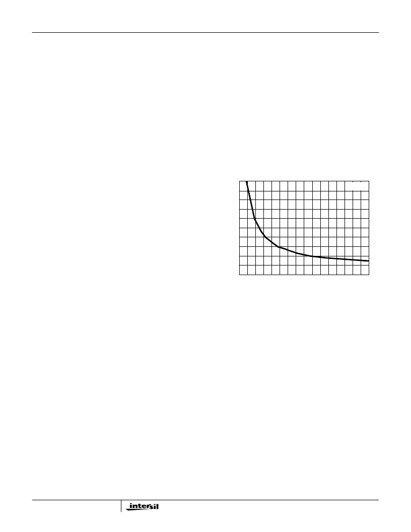
Driving Capacitive Loads
Capacitive loads, such as an A/D input, or an improperly
terminated transmission line will degrade the amplifier’s
phase margin resulting in frequency response peaking and
possible oscillations. In most cases, the oscillation can be
avoided by placing a resistor (R
S
) in series with the output
prior to the capacitance.
Figure 1 details starting points for the selection of this
resistor. The points on the curve indicate the R
S
and C
L
combinations for the optimum bandwidth, stability, and
settling time, but experimental fine tuning is recommended.
Picking a point above or to the right of the curve yields an
overdamped response, while points below or left of the curve
indicate areas of underdamped performance.
R
S
and C
L
form a low pass network at the output, thus
limiting system bandwidth well below the amplifier
bandwidth of 425MHz (for A
V
= +2). By decreasing R
S
as
C
L
increases (as illustrated in the curves), the maximum
bandwidth is obtained without sacrificing stability. In spite
of this, bandwidth still decreases as the load capacitance
increases. For example, at A
V
= +2, R
S
= 50
, C
L
= 22pF,
the overall bandwidth is limited to 230MHz, and bandwidth
drops to 80MHz at A
V
= +2, R
S
= 7
, C
L
= 390pF.
Evaluation Board
The performance of the HFA1205 may be evaluated using
the HA5023 Evaluation Board.
The performance of the HFA1205IB (SOIC) may be
evaluated using the HA5023 Evaluation Board and a SOIC
to DIP adaptor like the Aries Electronics Part Number
08-350000-10.
The schematic for amplifier 1 and the board layout are
shown in Figure 2 and Figure 3. Resistors R
F
, R
G
and R
S
may require a change to the appropriate value (see
“Optimum Feedback Resistor” section) for the gain being
evaluated.
To order evaluation boards (Part Number HA5023EVAL),
please contact your local sales office.
0
100
200
300
400
0
10
20
30
40
50
LOAD CAPACITANCE (pF)
S
)
A
V
= +2
150
250
350
50
FIGURE 1. RECOMMENDED SERIES OUTPUT RESISTOR vs
LOAD CAPACITANCE
HFA1205
相关PDF资料 |
PDF描述 |
|---|---|
| HFA120MD40C | Ultrafast, Soft Recovery Diode |
| HFA1212883 | 5.0V 216-mc CPLD - NOT RECOMMENDED for NEW DESIGN |
| HFA1212IB | Dual 350MHz, Low Power Closed Loop Buffer Amplifier |
| HFA1212IP | Dual 350MHz, Low Power Closed Loop Buffer Amplifier |
| HFA1212 | Dual 350MHz, Low Power Closed Loop Buffer Amplifier(350MHz、低功耗、输出限定锁相环缓冲器放大器) |
相关代理商/技术参数 |
参数描述 |
|---|---|
| HFA1205_04 | 制造商:INTERSIL 制造商全称:Intersil Corporation 功能描述:Dual, 425MHz, Low Power, Video Operational Amplifier |
| HFA1205IB | 制造商:Rochester Electronics LLC 功能描述:OPAMP 2X 400MHZ CFB 8SOIC IND - Bulk |
| HFA1205IP | 制造商:Rochester Electronics LLC 功能描述:OPAMP 2X 400MHZ CFB 8PDIP IND - Bulk |
| HFA120EA60 | 功能描述:DIODE HEXFRED 600V 75A SOT-227 RoHS:否 类别:半导体模块 >> 二极管,整流器 系列:HEXFRED® 标准包装:10 系列:- 电压 - 在 If 时为正向 (Vf)(最大):1.45V @ 30A 电流 - 在 Vr 时反向漏电:15µA @ 400V 电流 - 平均整流 (Io)(每个二极管):30A 电压 - (Vr)(最大):400V 反向恢复时间(trr):65ns 二极管类型:标准 速度:快速恢复 = 200mA(Io) 二极管配置:2 个独立式 安装类型:底座安装 封装/外壳:ISOTOP 供应商设备封装:ISOTOP? 包装:管件 |
| HFA120FA120P | 制造商:VISHAY 制造商全称:Vishay Siliconix 功能描述:HEXFRED Ultrafast Soft Recovery Diode, 120 A |
发布紧急采购,3分钟左右您将得到回复。