- 您现在的位置:买卖IC网 > PDF目录385375 > HFA1405 (Intersil Corporation) Quad, 675MHz, Low Power, Video Operational Amplifier(四路、675MHz低功耗视频运算放大器) PDF资料下载
参数资料
| 型号: | HFA1405 |
| 厂商: | Intersil Corporation |
| 英文描述: | Quad, 675MHz, Low Power, Video Operational Amplifier(四路、675MHz低功耗视频运算放大器) |
| 中文描述: | 四,675MHz,低功耗,视频运算放大器(四路,675MHz低功耗视频运算放大器) |
| 文件页数: | 5/15页 |
| 文件大小: | 330K |
| 代理商: | HFA1405 |
5
package type. Graphs not labeled with a specific package
type are applicable to all packages.
Optimum Feedback Resistor
Although a current feedback amplifier’s bandwidth
dependency on closed loop gain isn’t as severe as that of a
voltage feedback amplifier, there can be an appreciable
decrease in bandwidth at higher gains. This decrease may
be minimized by taking advantage of the current feedback
amplifier’s unique relationship between bandwidth and R
F
.
All current feedback amplifiers require a feedback resistor,
even for unity gain applications, and R
F
, in conjunction with
the internal compensation capacitor, sets the dominant pole
of the frequency response. Thus, the amplifier’s bandwidth is
inversely proportional to R
F
. The HFA1405 design is
optimized for R
F
= 402
/510
(PDIP/SOIC) at a gain of +2.
Decreasing R
F
decreases stability, resulting in excessive
peaking and overshoot (Note: Capacitive feedback causes
the same problems due to the feedback impedance
decrease at higher frequencies). However, at higher gains
the amplifier is more stable so R
F
can be decreased in a
trade-off of stability for bandwidth.
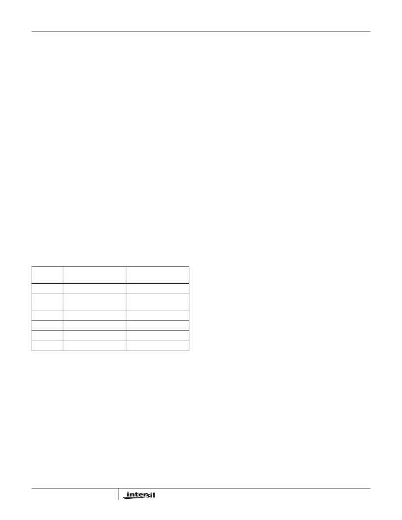
The table below lists recommended R
F
values for various
gains, and the expected bandwidth. For good channel-to-
channel gain matching, it is recommended that all resistors
(termination as well as gain setting) be
±
1% tolerance or
better.
NOTE:
the R
F
of the CLC414 and CLC415, for performance comparison
purposes. Performance at A
V
= +6 may be increased by reducing R
F
below 500
.
R
F
= 500
is not the optimum value. It was chosen to match
Non-inverting Input Source Impedance
For best operation, the DC source impedance seen by the
non-inverting input should be
≥
50
.
This is especially
important in inverting gain configurations where the non-
inverting input would normally be connected directly to GND.
Pulse Undershoot
The HFA1405 utilizes a quasi-complementary output stage
to achieve high output current while minimizing quiescent
supply current. In this approach, a composite device
replaces the traditional PNP pulldown transistor. The
composite device switches modes after crossing 0V,
resulting in added distortion for signals swinging below
ground, and an increased undershoot on the negative
portion of the output waveform (see Figure 6 and Figure 9).
This undershoot isn’t present for small bipolar signals, or
large positive signals (see Figure 4 and Figure 5).
PC Board Layout
The frequency response of this amplifier depends greatly on
the amount of care taken in designing the PC board.
The
use of low inductance components such as chip
resistors and chip capacitors is strongly recommended,
while a solid ground plane is a must!
Attention should be given to decoupling the power supplies.
A large value (10
μ
F) tantalum in parallel with a small value
(0.1
μ
F) chip capacitor works well in most cases.
Terminated microstrip signal lines are recommended at the
input and output of the device. Capacitance, parasitic or
planned, connected to the output must be minimized, or
isolated as discussed in the next section.
Care must also be taken to minimize the capacitance to
ground at the amplifier’s inverting input (-IN). The larger this
capacitance, the worse the gain peaking, resulting in pulse
overshoot and eventual instability. To reduce this
capacitance the designer should remove the ground plane
under traces connected to -IN, and keep connections to -IN
as short as possible.
An example of a good high frequency layout is the
Evaluation Board shown in Figure 3.
Driving Capacitive Loads
Capacitive loads, such as an A/D input, or an improperly
terminated transmission line will degrade the amplifier’s
phase margin resulting in frequency response peaking and
possible oscillations. In most cases, the oscillation can be
avoided by placing a resistor (R
S
) in series with the output
prior to the capacitance.
Figure 1 details starting points for the selection of this
resistor. The points on the curve indicate the R
S
and C
L
combinations for the optimum bandwidth, stability, and
settling time, but experimental fine tuning is recommended.
Picking a point above or to the right of the curve yields an
overdamped response, while points below or left of the curve
indicate areas of underdamped performance.
R
S
and C
L
form a low pass network at the output, thus limiting
system bandwidth well below the amplifier bandwidth of
560MHz. By decreasing R
S
as C
L
increases (as illustrated in
the curve), the maximum bandwidth is obtained without
sacrificing stability. In spite of this, bandwidth still decreases
as the load capacitance increases.
TABLE 1. OPTIMUM FEEDBACK RESISTOR
GAIN
(A
CL
)
R
F
(
)
PDIP/SOIC
BANDWIDTH (MHz)
PDIP/SOIC
-1
310/360
360/420
+1
510 (+R
S
= 510)/
464 (+R
S
= 649)
300/375
+2
402/510
400/560
+5
NA/200
NA/330
+6
500/500 (Note)
100/140
+10
NA/180
NA/140
HFA1405
相关PDF资料 |
PDF描述 |
|---|---|
| HFA140NJ60C | HEXFRED Ultrafast, Soft Recovery Diode |
| HFA1412 | Quad, 350MHz, Low Power, Programmable Gain Buffer Amplifier(四路、350MHz低功耗可编程增益缓冲器放大器) |
| HFA160MD40D | Ultrafast, Soft Recovery Diode |
| HFA160NJ40C | Ultrafast, Soft Recovery Diode |
| HFA16PA120C | HEXFRED Ultrafast, Soft Recovery Diode |
相关代理商/技术参数 |
参数描述 |
|---|---|
| HFA1405 WAF | 制造商:Harris Corporation 功能描述: 制造商:Intersil Corporation 功能描述: |
| HFA1405_05 | 制造商:INTERSIL 制造商全称:Intersil Corporation 功能描述:Quad, 560MHz, Low Power, Video Operational Amplifier |
| HFA1405IA | 制造商:Rochester Electronics LLC 功能描述:- Bulk |
| HFA1405IB | 制造商:Intersil Corporation 功能描述: |
| HFA1405IB96 | 制造商:未知厂家 制造商全称:未知厂家 功能描述:Current-Feedback Operational Amplifier |
发布紧急采购,3分钟左右您将得到回复。