- 您现在的位置:买卖IC网 > PDF目录385375 > HFA1412 (Intersil Corporation) Quad, 350MHz, Low Power, Programmable Gain Buffer Amplifier(四路、350MHz低功耗可编程增益缓冲器放大器) PDF资料下载
参数资料
| 型号: | HFA1412 |
| 厂商: | Intersil Corporation |
| 英文描述: | Quad, 350MHz, Low Power, Programmable Gain Buffer Amplifier(四路、350MHz低功耗可编程增益缓冲器放大器) |
| 中文描述: | 四,350MHz的,低功耗,可编程增益缓冲放大器(四路,350MHz的低功耗可编程增益缓冲器放大器) |
| 文件页数: | 5/13页 |
| 文件大小: | 332K |
| 代理商: | HFA1412 |
5
FN4152.4
January 23, 2006
Application Information
HFA1412 Advantages
The HFA1412 features a novel design which allows the user
to select from three closed loop gains, without any external
components. The result is a more flexible product, fewer part
types in inventory, and more efficient use of board space.
Implementing a quad, gain of 2, cable driver with this IC
eliminates the eight gain setting resistors, which frees up
board space for termination resistors.
Like most newer high performance amplifiers, the HFA1412
is a current feedback amplifier (CFA). CFAs offer high
bandwidth and slew rate at low supply currents, but can be
difficult to use because of their sensitivity to feedback
capacitance and parasitics on the inverting input (summing
node). The HFA1412 eliminates these concerns by bringing
the gain setting resistors on-chip. This yields the optimum
placement and value of the feedback resistor, while
minimizing feedback and summing node parasitics. Because
there is no access to the summing node, the PCB parasitics
do not impact performance at gains of +2 or -1 (see “Unity
Gain Considerations” for discussion of parasitic impact on
unity gain performance).
The HFA1412’s closed loop gain implementation provides
better gain accuracy, lower offset and output impedance,
and better distortion compared with open loop buffers.
Closed Loop Gain Selection
This “buffer” operates in closed loop gains of -1, +1, or +2, with
gain selection accomplished via connections to the
±
inputs.
Applying the input signal to +IN and floating -IN selects a gain
of +1 (see next section for layout caveats), while grounding -IN
selects a gain of +2. A gain of -1 is obtained by applying the
input signal to -IN with +IN grounded through a 50
resistor.
The table below summarizes these connections:
Unity Gain Considerations
Unity gain selection is accomplished by floating the -Input of
the HFA1412. Anything that tends to short the -Input to GND,
such as stray capacitance at high frequencies, will cause the
amplifier gain to increase toward a gain of +2. The result is
excessive high frequency peaking, and possible instability.
Even the minimal amount of capacitance associated with
attaching the -Input lead to the PCB results in approximately
6dB of gain peaking. At a minimum this requires due care to
ensure the minimum capacitance at the -Input connection.
Table 1 lists five alternate methods for configuring the
HFA1412 as a unity gain buffer, and the corresponding
performance. The implementations vary in complexity and
involve performance trade-offs. The easiest approach to
implement is simply shorting the two input pins together, and
applying the input signal to this common node. The amplifier
bandwidth decreases from 550MHz to 370MHz, but
excellent gain flatness is the benefit. A drawback to this
approach is that the amplifier input noise voltage and input
offset voltage terms see a gain of +2, resulting in higher
noise and output offset voltages. Alternately, a 100pF
capacitor between the inputs shorts them only at high
frequencies, which prevents the increased output offset
voltage but delivers less gain flatness.
Another straightforward approach is to add a 620
resistor
in series with the amplifier’s positive input. This resistor and
the HFA1412 input capacitance form a low pass filter which
rolls off the signal bandwidth before gain peaking occurs.
This configuration was employed to obtain the data sheet AC
and transient parameters for a gain of +1.
Pulse Overshoot
The HFA1412 utilizes a quasi-complementary output stage
to achieve high output current while minimizing quiescent
supply current. In this approach, a composite device
replaces the traditional PNP pulldown transistor. The
composite device switches modes after crossing 0V,
resulting in added distortion for signals swinging below
ground, and an increased overshoot on the negative portion
of the output waveform (see Figure 5, Figure 7, and Figure 9).
This overshoot isn’t present for small bipolar signals (see
Figure 4, Figure 6, and Figure 8) or large positive signals.
Figure 28 through Figure 31 illustrate the amplifier’s
overshoot dependency on input transition time, and signal
polarity.
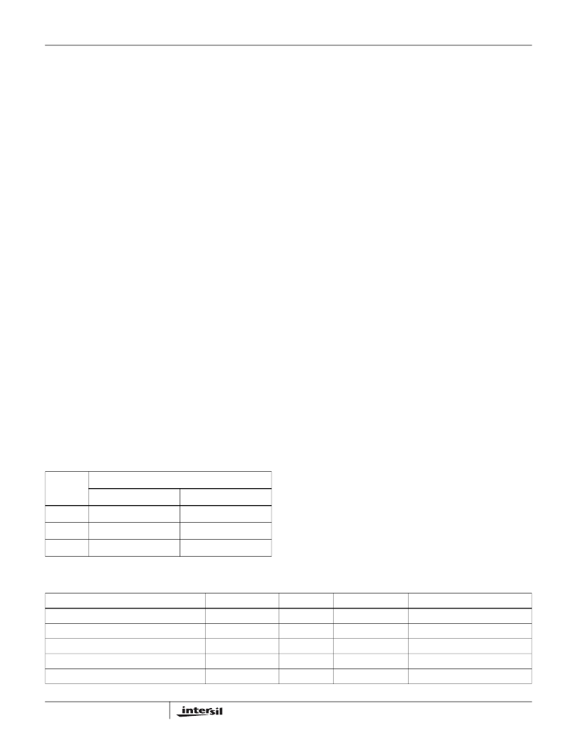
GAIN
(A
CL
)
CONNECTIONS
+INPUT
-INPUT
-1
50
to GND
Input
+1
Input
NC (Floating)
+2
Input
GND
TABLE 1. UNITY GAIN PERFORMANCE FOR VARIOUS IMPLEMENTATIONS
APPROACH
PEAKING (dB)
BW (MHz)
SR (V/
μ
s)
±
0.1dB GAIN FLATNESS (MHz)
Remove -IN Pin
5.0
550
1300
18
+R
S
= 620
1.0
230
1000
25
+R
S
= 620
and Remove -IN Pin
0.7
225
1000
28
Short +IN to -IN (e.g., Pins 2 and 3)
0.1
370
500
170
100pF Capacitor Between +IN and -IN
0.3
380
550
130
HFA1412
相关PDF资料 |
PDF描述 |
|---|---|
| HFA160MD40D | Ultrafast, Soft Recovery Diode |
| HFA160NJ40C | Ultrafast, Soft Recovery Diode |
| HFA16PA120C | HEXFRED Ultrafast, Soft Recovery Diode |
| HFA16TA60C | Ultrafast, Soft Recovery Diode |
| HFA180NH40R | Ultrafast, Soft Recovery Diode |
相关代理商/技术参数 |
参数描述 |
|---|---|
| HFA1412/883 | 制造商:INTERSIL 制造商全称:Intersil Corporation 功能描述:Quad, High Speed, Low Power, Video Closed Loop Buffer |
| HFA1412_06 | 制造商:INTERSIL 制造商全称:Intersil Corporation 功能描述:Quad, 350MHz, Low Power, Programmable Gain Buffer Amplifier |
| HFA1412IB | 功能描述:IC BUFFER QUAD 350MHZ LP 14-SOIC RoHS:否 类别:集成电路 (IC) >> Linear - Amplifiers - Instrumentation 系列:- 标准包装:50 系列:LinCMOS™ 放大器类型:通用 电路数:4 输出类型:- 转换速率:0.05 V/µs 增益带宽积:110kHz -3db带宽:- 电流 - 输入偏压:0.7pA 电压 - 输入偏移:210µV 电流 - 电源:57µA 电流 - 输出 / 通道:30mA 电压 - 电源,单路/双路(±):3 V ~ 16 V,±1.5 V ~ 8 V 工作温度:-40°C ~ 85°C 安装类型:表面贴装 封装/外壳:14-SOIC(0.154",3.90mm 宽) 供应商设备封装:14-SOIC 包装:管件 产品目录页面:865 (CN2011-ZH PDF) 其它名称:296-1834296-1834-5 |
| HFA1412IBZ | 功能描述:特殊用途放大器 W/ANNEAL BUFR 4X 350 MHZ PRG GAIN 14 IND RoHS:否 制造商:Texas Instruments 通道数量:Single 共模抑制比(最小值): 输入补偿电压: 工作电源电压:3 V to 5.5 V 电源电流:5 mA 最大功率耗散: 最大工作温度:+ 70 C 最小工作温度:- 40 C 安装风格:SMD/SMT 封装 / 箱体:QFN-20 封装:Reel |
| HFA1412IP | 功能描述:IC BUFFER QUAD 350MHZ LP 14-DIP RoHS:否 类别:集成电路 (IC) >> Linear - Amplifiers - Instrumentation 系列:- 标准包装:50 系列:LinCMOS™ 放大器类型:通用 电路数:4 输出类型:- 转换速率:0.05 V/µs 增益带宽积:110kHz -3db带宽:- 电流 - 输入偏压:0.7pA 电压 - 输入偏移:210µV 电流 - 电源:57µA 电流 - 输出 / 通道:30mA 电压 - 电源,单路/双路(±):3 V ~ 16 V,±1.5 V ~ 8 V 工作温度:-40°C ~ 85°C 安装类型:表面贴装 封装/外壳:14-SOIC(0.154",3.90mm 宽) 供应商设备封装:14-SOIC 包装:管件 产品目录页面:865 (CN2011-ZH PDF) 其它名称:296-1834296-1834-5 |
发布紧急采购,3分钟左右您将得到回复。