- 您现在的位置:买卖IC网 > PDF目录385378 > HI-1575PCI (HOLT INTEGRATED CIRCUITS INC) 3.3V Dual Transceivers with Integrated Encoder / Decoders PDF资料下载
参数资料
| 型号: | HI-1575PCI |
| 厂商: | HOLT INTEGRATED CIRCUITS INC |
| 元件分类: | 网络接口 |
| 英文描述: | 3.3V Dual Transceivers with Integrated Encoder / Decoders |
| 中文描述: | DATACOM, MIL-STD-1553 DATA BUS TRANSCEIVER, PQCC40 |
| 封装: | 6 X 6 MM, PLASTIC PACKAGE-40 |
| 文件页数: | 2/12页 |
| 文件大小: | 128K |
| 代理商: | HI-1575PCI |
HOLT INTEGRATED CIRCUITS
2
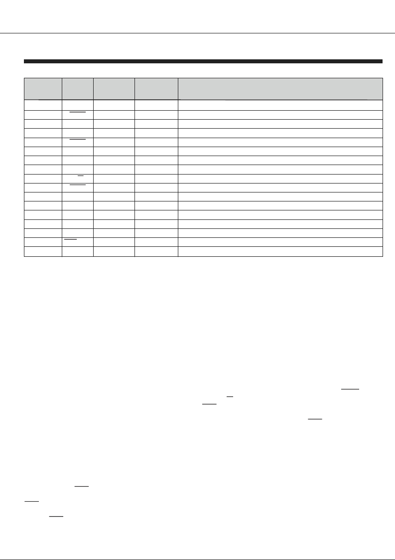
PIN
SYMBOL FUNCTION
PULL-UP
PULL-DOWN
DESCRIPTION
(TQFP)
1
RCVA
Digital output
-
Goes high when MIL-STD-1553 word received on Bus A
2
3
4
5,
6
7
8
REG
BUSA
BUSB
W
STRB
CHA
Analog I/O
-
MIL-STD-1533 bus driver A, negative signal
BUSA
Analog I/O
-
MIL-STD-1553 bus driver A, positive signal
VDD
Power supply
-
+3.3 VDCr
Analog I/O
-
MIL-STD-1533 bus driver B, negative signal
BUSB
Analog I/O
-
MIL-STD-1553 bus driver B, positive signal
RCVB
Digital output
-
Goes high when MIL-STD-1553 word received on Bus B
Digital input
12K pull-down
Selects Status & Mode Register when high, or Data registers when low
9
R/
Digital input
12K pull-up
Controls data and sync direction during read or write operations
10
Digital input
12K pull-up
Strobe. Timing input to control register read and write operations
11
MR
Digital input
12K pull-down
Pulse high to reset the HI-1575
12
SYNC
Digital I/O
12K pull-down
Selects transmit sync type on write, indicates received sync type on read.
13-20, 22-29
D15:D0
Digital I/O
12K pull-down
Data bus. D15 (MSB) corresponds to MIL-STD-1553 bit 4
21
GND
Power supply
-
Ground
30
CLK
Digital input
-
12 MHz clock
31
/CHB
Digital Input
12K pull-down
Selects MIL-STD-1553 Bus A or Bus B
32
ERROR
Digital output
-
Goes high when a received MIL-STD-1553 word has an encoding error
PIN DESCRIPTIONS
FUNCTIONAL DESCRIPTION
Figure1showsasimplifiedblockdiagramoftheHI-1575.
The MR (Master Reset) input should be pulsed high to
initialize the Manchester II Encoder and Decoders. MR
also clears the Receive Data registers, RXA and RXB,
and sets the Status & Mode register to its default state as
described in figure 2.
The CLK input requires a 12.0 MHz clock signal. CLK is
used to derive the 1.0 us bit period for MIL-STD-1553
data transmission, as well to provide the master clock for
the Manchester II encoder and the decoder's receiver
sampling logic.
The HI-1575 is configured by writing bits 0 - 5 of the Sta-
tus & Mode (SAM) register. Refer to figure 2 for a com-
plete description. SAM bits 0 - 5 are read/write allowing
the user to verify the chip's configuration at any time by
reading the SAM. SAM is accessed by performing a read
or write cycle with the REG input high.
SAM bits 6 - 15 are read-only and are used to provide
status information.
To allow the user to minimize the number of hardware
control inputs, SAM bit 5 (Channel A/B select) is logically
'OR'ed with the
/CHB input pin. To select between
MIL-STD-1553 bus A or B, the user may either tie the
/CHB pin low and select buses using SAM bit 5
(software control), or program SAM bit 5 to a zero and
use the
/CHB pin to select the active bus (hardware
control).
STATUS&MODEREGISTER
CHA
CHA
CHA
Similarly, the SYNC I/O pin may be left open-circuit al-
lowing the transmitter sync to be programmed into SAM
bit 4, or SAM bit 4 can be set to zero and the SYNC pin
used to set the transmitted SYNC type. Note that SYNC
is an I/O pin. It is an input when writing data to the
HI-1575 transmit data register (TX), and an output when
reading data from the HI-1575 receivers (RXA and RXB).
The SYNC pin must not be shorted directly to VDD or
GND. An internal pull-down resistor allow the SYNC pin
to be left open-circuit if the user opts for purely software
control.
Data words to be transmitted on the MIL-STD-1553 data
bus are written to the TX register by pulsing
while R/
is low and REG is low. The logical OR of the
/CHB input pin and SAM bit 5 (CHAN) during the
write cycle determines whether the word is output on
MIL-STD-1553 bus A or B. Setting
to a zero selects bus A, and a one selects bus B. The log-
ical OR of the SYNC pin and SAM bit 4 (TXSYNC) dur-
ing the write cycle defines whether the transmitted word
is a MIL-STD-1553 Command or Data word. Setting
SYNC to a one causes a Command (or Status) sync to
be generated. Setting SYNC to zero selects a Data sync.
Note that the SYNC pin is bidirectional. It should be
treated as an extension to the 16-bit bidirectional
databus (D15:D0) in terms of I/O switching and timing.
low
/CHB OR CHAN
CHA
TheHI-1575automaticallycalculatesandappendsthecor-
rect parity bit to the transmitted word. Each word is as-
signedoddparityasrequiredbyMIL-STD-1553.
TRANSMITTER
STRB
W
CHA
HI-1575
相关PDF资料 |
PDF描述 |
|---|---|
| HI-1575PCIF | 3.3V Dual Transceivers with Integrated Encoder / Decoders |
| HI-1575PCM | 3.3V Dual Transceivers with Integrated Encoder / Decoders |
| HI-1575PCMF | 3.3V Dual Transceivers with Integrated Encoder / Decoders |
| HI-1575PCT | 3.3V Dual Transceivers with Integrated Encoder / Decoders |
| HI-1575PCTF | 3.3V Dual Transceivers with Integrated Encoder / Decoders |
相关代理商/技术参数 |
参数描述 |
|---|---|
| HI-1575PCIF | 制造商:HOLTIC 制造商全称:Holt Integrated Circuits 功能描述:3.3V Dual Transceivers with Integrated Encoder / Decoders |
| HI-1575PCM | 制造商:HOLTIC 制造商全称:Holt Integrated Circuits 功能描述:3.3V Dual Transceivers with Integrated Encoder / Decoders |
| HI-1575PCMF | 制造商:HOLTIC 制造商全称:Holt Integrated Circuits 功能描述:3.3V Dual Transceivers with Integrated Encoder / Decoders |
| HI-1575PCT | 制造商:HOLTIC 制造商全称:Holt Integrated Circuits 功能描述:3.3V Dual Transceivers with Integrated Encoder / Decoders |
| HI-1575PCTF | 制造商:HOLTIC 制造商全称:Holt Integrated Circuits 功能描述:3.3V Dual Transceivers with Integrated Encoder / Decoders |
发布紧急采购,3分钟左右您将得到回复。