- 您现在的位置:买卖IC网 > PDF目录385379 > HI1166Y (Intersil Corporation) 8-Bit 250 MSPS Flash A/D Converter PDF资料下载
参数资料
| 型号: | HI1166Y |
| 厂商: | Intersil Corporation |
| 英文描述: | 8-Bit 250 MSPS Flash A/D Converter |
| 中文描述: | 8位250 MSPS的闪光的A / D转换器 |
| 文件页数: | 3/8页 |
| 文件大小: | 585K |
| 代理商: | HI1166Y |
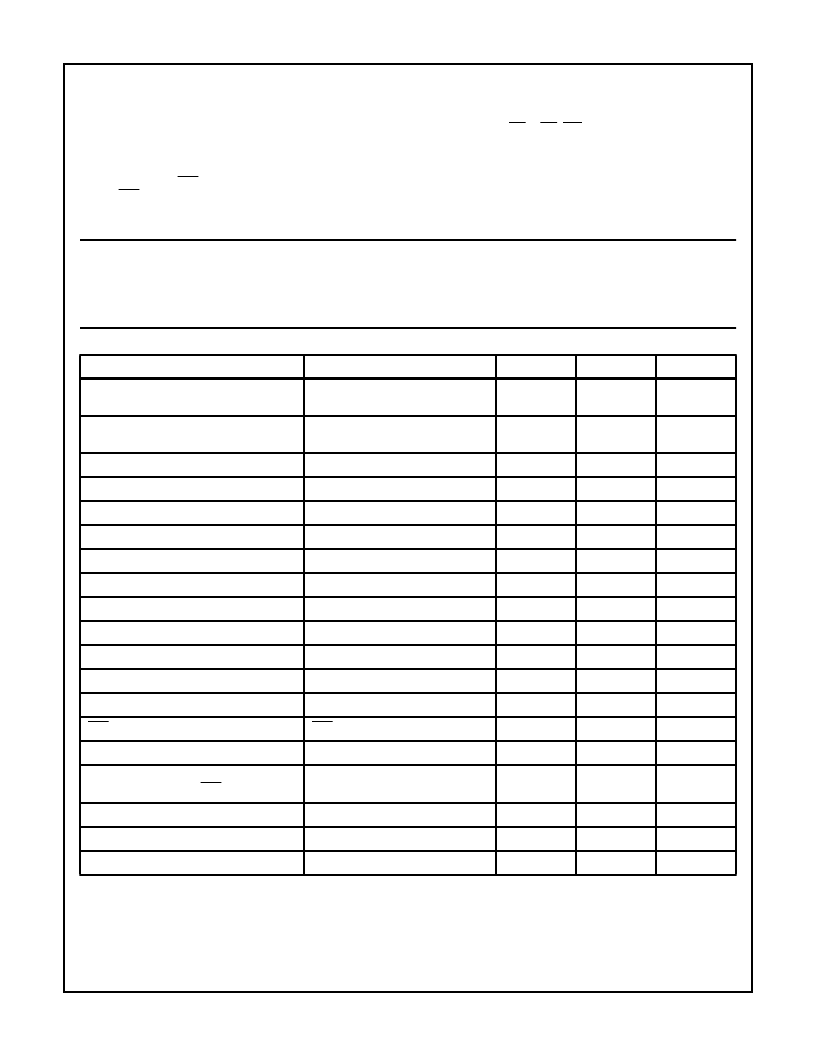
3
Specifications HI1166Y
Absolute Maximum Ratings
T
A
= +25
o
C
Supply Voltage (AV
EE
, DV
EE
). . . . . . . . . . . . . . . . . . . . -7V to +0.5V
Analog Input Voltage (V
IN
) . . . . . . . . . . . . . . . . . . . . . -2.7V to +0.5V
Reference Input Voltage
V
RT
, V
RB
, V
RM
. . . . . . . . . . . . . . . . . . . . . . . . . . . . . -2.7V to +0.5V
|V
RT
-V
RB
|. . . . . . . . . . . . . . . . . . . . . . . . . . . . . . . . . . . . . . . .2.5V
Digital Input Voltage
MINV, LINV, CLK, CLK . . . . . . . . . . . . . . . . . . . . . . . -4V to +0.5V
|CLK-CLK| . . . . . . . . . . . . . . . . . . . . . . . . . . . . . . . . . . . . . . .2.7V
V
RM
Pin Input Current (I
VRM
) . . . . . . . . . . . . . . . . . . .-3mA to +3mA
Digital Output Current
(ID0 to ID7, IOR, ID0 to ID7, IOR). . . . . . . . . . . . . .-30mA to 0mA
Storage Temperature Range (T
STG
) . . . . . . . . . . . .-65
o
C to +150
o
C
CAUTION: Stresses above those listed in “Absolute Maximum Ratings” may cause permanent damage to the device. This is a stress only rating and operation
of the device at these or any other conditions above those indicated in the operational sections of this specification is not implied.
Operating Conditions
Supply Voltage
AV
EE
, DV
EE
. . . . . . . . . . . . . . . . . . . . . . . . . . . . . . -5.5V to -4.95V
AV
EE
- DV
EE
. . . . . . . . . . . . . . . . . . . . . . . . . . . . . -0.05V to 0.05V
AGND - DGND . . . . . . . . . . . . . . . . . . . . . . . . . . . -0.05V to 0.05V
Reference Input Voltage
V
RT
. . . . . . . . . . . . . . . . . . . . . . . . . . . . . . . . . . . . . .-0.1V to 0.1V
V
RB
. . . . . . . . . . . . . . . . . . . . . . . . . . . . . . . . . . . . . -2.2V to -1.8V
Analog Input Voltage, V
IN
. . . . . . . . . . . . . . . . . . . . . . . . V
RB
to V
RT
Electrical Specifications
T
A
= +25
o
C, DV
EE
, AV
EE
= -5.2V, V
RT
= 0V, V
RB
= -2V
PARAMETER
TEST CONDITIONS
MIN
MAX
UNIT
Differential Linearity Error (DNL)
(00000000 to 11111111)
-0.7
0.7
LSB
Integral Linearity Error (INL)
(00000000 to 11111111)
-0.7
0.7
LSB
Resolution
8
-
Bits
Input Bias Current, L
IN
V
IN
= -1.0V
35
400
μ
A
Analog Input Resistance, R
IN
V
IN
= -1.0V
55
350
k
Resister-String Current, I
REF
-24
-13
mA
Reference Voltage, V
RM
-1.1
-0.9
V
Residual Resistance, R1
0.1
1.2
Residual Resistance, R2
380
620
Residual Resistance, R5
0.1
1.2
Residual Resistance, R4
380
620
Digital Input Current HI, I
IH
Hi = -0.8V
0
40
μ
A
Digital Input Current LO, I
IL
Lo = -1.6V
-30
30
μ
A
CLK Open Voltage, V
OPN
CLK = Open
-1.4
-1.2
V
Leakage (1) D0 to D7, V
LEAK
I = -10
μ
A
-1.0
-0.3
V
Leakage (2) D0 to D7,
VIN, LINV, MINV, CLK, CLK, I
LEAK
V = 0.3V
-1.0
1.0
μ
A
Digital Output Voltage HI, V
OH
620
to -5.2V
-1
-0.6
V
Digital Output Voltage LO, V
OL
620
to -5.2V
-2
-1.55
V
Supply Current, I
EE
-330
-190
mA
相关PDF资料 |
PDF描述 |
|---|---|
| HI1166 | 8-Bit, 250 MSPS, Flash A/D Converter(8位、250MSPS低功耗 、闪速 A/D转换器) |
| HI13003 | NPN EPITAXIAL PLANAR TRANSISTOR |
| HI1386Y | 8-Bit, 75 MSPS Flash A/D Converter |
| HI1386 | 8-Bit, 75 MSPS, Flash A/D Converter |
| HI1386AIL | 8-Bit, 75 MSPS, Flash A/D Converter |
相关代理商/技术参数 |
参数描述 |
|---|---|
| HI117 | 制造商:HSMC 制造商全称:HSMC 功能描述:PNP EPITAXIAL PLANAR TRANSISTOR |
| HI1171 | 制造商:INTERSIL 制造商全称:Intersil Corporation 功能描述:8位, 40个中型项目,高速D / A转换器 |
| HI1171_05 | 制造商:INTERSIL 制造商全称:Intersil Corporation 功能描述:8-Bit, 40 MSPS, High Speed D/A Converter |
| HI1171-EV | 制造商:Intersil Corporation 功能描述:EVAL BD FOR HI1171 - Bulk |
| HI1171JCB | 功能描述:IC DAC 8BIT 40MSPS HS 24-SOIC RoHS:是 类别:集成电路 (IC) >> 数据采集 - 数模转换器 系列:- 标准包装:2,400 系列:- 设置时间:- 位数:18 数据接口:串行 转换器数目:3 电压电源:模拟和数字 功率耗散(最大):- 工作温度:-40°C ~ 85°C 安装类型:表面贴装 封装/外壳:36-TFBGA 供应商设备封装:36-TFBGA 包装:带卷 (TR) 输出数目和类型:* 采样率(每秒):* |
发布紧急采购,3分钟左右您将得到回复。