参数资料
| 型号: | HI1171JCB-T |
| 厂商: | Intersil |
| 文件页数: | 3/7页 |
| 文件大小: | 0K |
| 描述: | CONV D/A 8BIT 40MSPS HS 24-SOIC |
| 标准包装: | 1,000 |
| 设置时间: | 10ns |
| 位数: | 8 |
| 数据接口: | 并联 |
| 转换器数目: | 1 |
| 电压电源: | 模拟和数字 |
| 功率耗散(最大): | 80mW |
| 工作温度: | -40°C ~ 85°C |
| 安装类型: | 表面贴装 |
| 封装/外壳: | 24-SOIC(0.209",5.30mm 宽) |
| 供应商设备封装: | 24-SOIC W |
| 包装: | 带卷 (TR) |
| 输出数目和类型: | 2 电流,单极 |
| 采样率(每秒): | 40M |
3
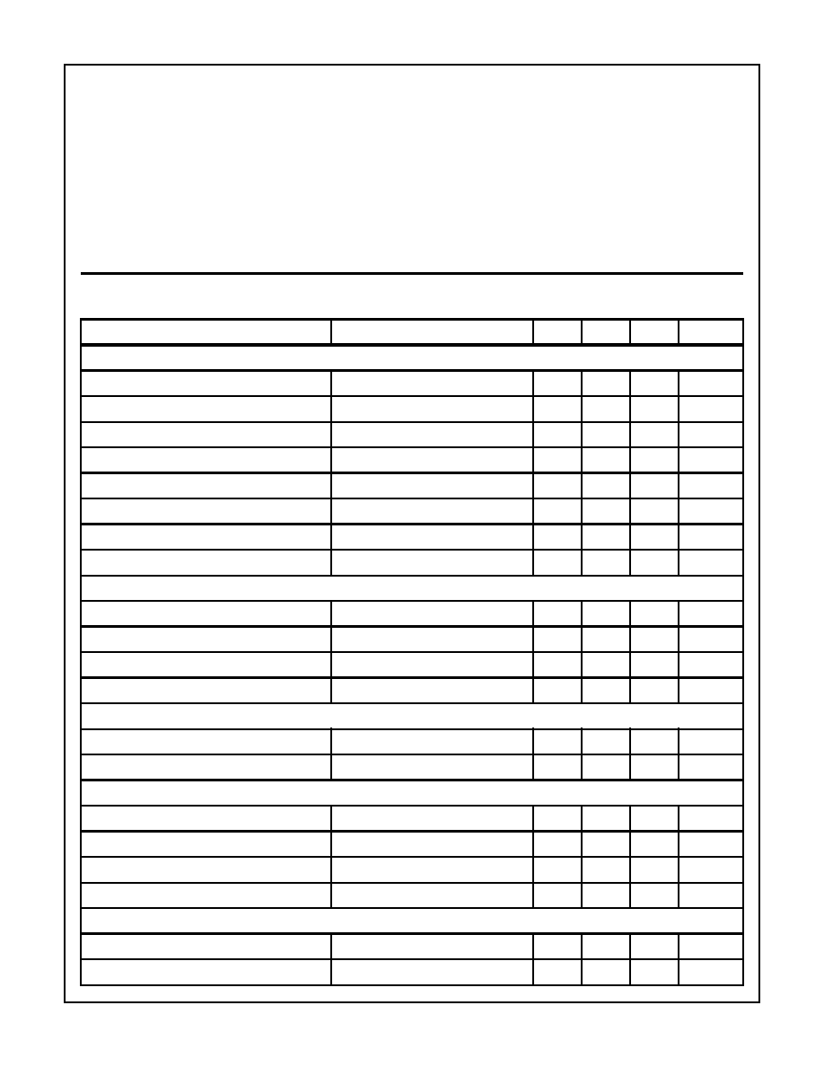
Absolute Maximum Ratings
Thermal Information
Digital Supply Voltage DVDD to DVSS . . . . . . . . . . . . . . . . . . +7.0V
Analog Supply Voltage AVDD to AVSS . . . . . . . . . . . . . . . . . . +7.0V
Input Voltage . . . . . . . . . . . . . . . . . . . . . . . . . . . . . . . VDD to VSS V
Output Current . . . . . . . . . . . . . . . . . . . . . . . . . . . . . . .0mA to 15mA
Operating Conditions
Temperature Range . . . . . . . . . . . . . . . . . . . . . . . . . . -40oC to 85oC
Thermal Resistance (Typical, Note 1)
θJA (oC/W)
SOIC Package. . . . . . . . . . . . . . . . . . . . . . . . . . . . .
98
Maximum Junction Temperature, Plastic Package . . . . . . . . 150oC
Maximum Storage Temperature Range . . . . . . . . . . -65oC to 150oC
Maximum Lead Temperature (Soldering 10s). . . . . . . . . . . . 300oC
(SOIC - Lead Tips Only)
CAUTION: Stresses above those listed in “Absolute Maximum Ratings” may cause permanent damage to the device. This is a stress only rating and operation
of the device at these or any other conditions above those indicated in the operational sections of this specification is not implied.
NOTE:
1.
θJA is measured with the component mounted on an evaluation PC board in free air.
Electrical Specifications
AVDD = +4.75V to +5.25V, DVDD = +4.75 to +5.25V, VREF = +2.0V, fS = 40MHz,
CLK Pulse Width = 12.5ns, TA = 25
oC (Note 4)
PARAMETER
TEST CONDITIONS
MIN
TYP
MAX
UNITS
SYSTEM PERFORMANCE
Resolution, n
-8-
Bits
Integral Linearity Error, INL
fS = 40MHz (End Point)
-0.5
-
1.3
LSB
Differential Linearity Error, DNL
fS = 40MHz
-
±0.25
LSB
Offset Error, VOS
(Note 2)
-
1
mV
Full Scale Error, FSE (Adjustable to Zero)
(Note 2)
-
±13
LSB
Full Scale Output Current, IFS
-10
15
mA
Full Scale Output Voltage, VFS
1.9
2.0
2.1
V
Output Voltage Range, VFSR
0.5
2.0
2.1
V
DYNAMIC CHARACTERISTICS
Throughput Rate
See Figure 7
40.0
-
MHz
Glitch Energy, GE
ROUT = 75
-30-
pV-s
Differential Gain,
AV (Note 3)
-
1.2
-
%
Differential Phase,
φ (Note 3)
-
0.5
-
Degree
REFERENCE INPUT
Voltage Reference Input Range
0.5
-
2.0
V
Reference Input Resistance
(Note 3)
1.0
-
M
DIGITAL INPUTS
Input Logic High Voltage, VIH
(Note 3)
3.0
-
V
Input Logic Low Voltage, VIL
(Note 3)
-
1.5
V
Input Logic Current, IIL, IIH
(Note 3)
-
±5.0
A
Digital Input Capacitance, CIN
(Note 3)
-
5.0
-
pF
TIMING CHARACTERISTICS
Data Setup Time, tSU
See Figure 1
5
-
ns
Data Hold Time, tHLD
See Figure 1
10
-
ns
HI1171
相关PDF资料 |
PDF描述 |
|---|---|
| HI1175JCB-T | CONV A/D 8BIT 20MSPS 24-SOIC |
| HI1178JCQ | CONV D/A 8BIT TRPL 40MHZ 48-PQFP |
| HI3-674AKN-5 | IC ADC 12BIT 67KSPS 28-SBDIP |
| HI3-7159A-5Z | IC ADC 5-1/2 DIGIT 28-PDIP |
| HI3-DAC80V-5 | CONV D/A 12BIT OUTPUT AMP 24PDIP |
相关代理商/技术参数 |
参数描述 |
|---|---|
| HI1172 | 制造商:INTERSIL 制造商全称:Intersil Corporation 功能描述:6-Bit, 20 MSPS,Video A/D Converter (CMOS) |
| HI1172_00 | 制造商:INTERSIL 制造商全称:Intersil Corporation 功能描述:6-Bit, 20MSPS, Video A/D Converter (CMOS) |
| HI1172JCB | 制造商:Rochester Electronics LLC 功能描述:16 SOIC COMTEMP VIDEO A/D 6BIT 20MSPS - Bulk |
| HI1172JCB-T | 制造商:Rochester Electronics LLC 功能描述:- Tape and Reel |
| HI1172JCP | 制造商:Rochester Electronics LLC 功能描述:- Bulk 制造商:Harris Corporation 功能描述: |
发布紧急采购,3分钟左右您将得到回复。