- 您现在的位置:买卖IC网 > PDF目录11418 > HI3-0516-5Z (Intersil)IC MULTIPLEXER 16X1 28DIP PDF资料下载
参数资料
| 型号: | HI3-0516-5Z |
| 厂商: | Intersil |
| 文件页数: | 4/8页 |
| 文件大小: | 0K |
| 描述: | IC MULTIPLEXER 16X1 28DIP |
| 标准包装: | 13 |
| 功能: | 多路复用器 |
| 电路: | 1 x 16:1 |
| 导通状态电阻: | 750 欧姆 |
| 电压电源: | 双电源 |
| 电压 - 电源,单路/双路(±): | ±15V |
| 电流 - 电源: | 30mA |
| 工作温度: | 0°C ~ 75°C |
| 安装类型: | 通孔 |
| 封装/外壳: | 28-DIP(0.600",15.24mm) |
| 供应商设备封装: | 28-PDIP |
| 包装: | 管件 |
| 产品目录页面: | 1242 (CN2011-ZH PDF) |
4
Absolute Maximum Ratings
Thermal Information
V+ to V- . . . . . . . . . . . . . . . . . . . . . . . . . . . . . . . . . . . . . . . . . . . 33V
Analog Signal. . . . . . . . . . . . . . . . . . . . . . . . . . . . . . . . . (VIN, VOUT)
. . . . . . . . . . . . . . . . . . . . . . . . . . . . . . . . . . . . . . (V-) -2V to (V+) +2V
Digital Input Voltage:
TTL Levels Selected (VDD/LLS Pin = GND or Open)
VA0-2 . . . . . . . . . . . . . . . . . . . . . . . . . . . . . . . . . . . . . . -6V to +6V
VA3/SDS. . . . . . . . . . . . . . . . . . . . . . . . . . . . . (V-) -2V to (V+) +2V
CMOS Levels Selected (VDD/LLS Pin = VDD)
VA0-3 . . . . . . . . . . . . . . . . . . . . . . . . . . . . . . . . . . -2V to (V+) +2V
Operating Conditions
Temperature Ranges
HI-516-5 . . . . . . . . . . . . . . . . . . . . . . . . . . . . . . . . . . 0oC to 75oC
Thermal Resistance (Typical, Note 2)
θJA (oC/W)
PDIP Package* . . . . . . . . . . . . . . . . . . . . . . . . . . . .
60
Maximum Junction Temperature
Plastic Package . . . . . . . . . . . . . . . . . . . . . . . . . . . . . . . . . . 150oC
Maximum Storage Temperature Range . . . . . . . . . -65oC to 150oC
Maximum Lead Temperature (Soldering 10s) . . . . . . . . . . . . . 300oC
*Pb-free PDIPs can be used for through hole wave solder processing
only. They are not intended for use in Reflow solder processing
applications.
CAUTION: Stresses above those listed in “Absolute Maximum Ratings” may cause permanent damage to the device. This is a stress only rating and operation of the
device at these or any other conditions above those indicated in the operational sections of this specification is not implied.
NOTE:
2.
θJA is measured with the component mounted on an evaluation PC board in free air.
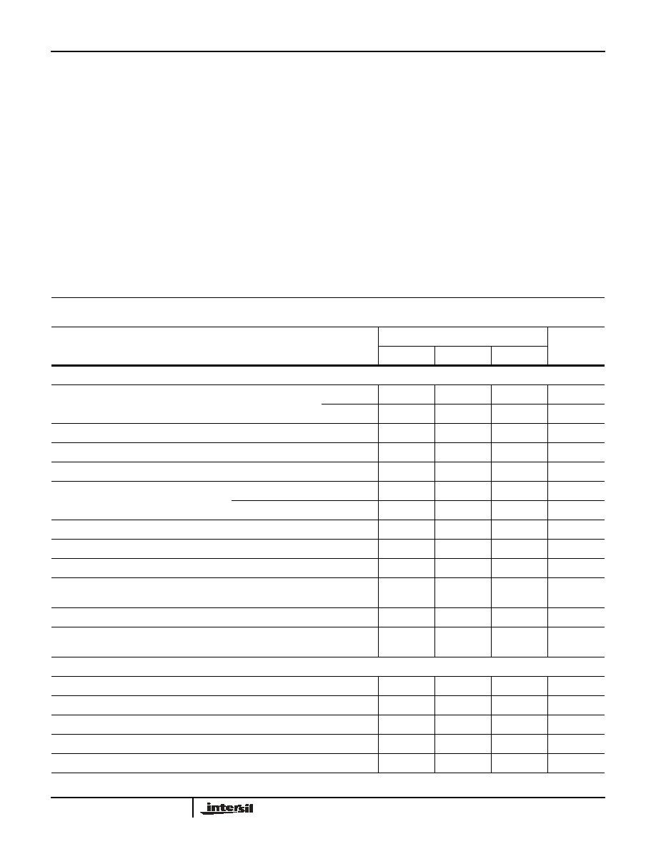
Electrical Specifications
Supplies = +15V, -15V; VAH (Logic Level High) = 2.4V, VAL (Logic Level Low) = 0.8V;
VDD/LLS = GND. (Note 3) Unless Otherwise Specified
PARAMETER
TEST
CONDITIONS
TEMP
(oC)
-5
UNITS
MIN
TYP
MAX
DYNAMIC CHARACTERISTICS
Access Time, tA
25
-
130
175
ns
Full
-
225
ns
Break-Before-Make Delay, tOPEN
25
10
20
-
ns
Enable Delay (ON), tON(EN)
25
-
120
175
ns
Enable Delay (OFF), tOFF(EN)
25
-
140
175
ns
Settling Time
To 0.1%
25
-
250
-
ns
To 0.01%
25
-
800
-
ns
Charge Injection Error
Note 6
25
-
20
mV
Off Isolation
Note 7
25
55
-
dB
Channel Input Capacitance, CS(OFF)
25
-
10
pF
Channel Output Capacitance,
CD(OFF)
25
-
25
pF
Digital Input Capacitance, CA
25
-
10
pF
Input to Output Capacitance,
CDS(OFF)
25
-
0.02
-
pF
DIGITAL INPUT CHARACTERISTICS
Input Low Threshold, VAL (TTL)
Note 3
Full
-
0.8
V
Input High Threshold, VAH (TTL)
Note 3
Full
2.4
-
V
Input Low Threshold, VAL (CMOS)
Note 3
Full
-
0.3VDD
V
Input High Threshold, VAH (CMOS)
Note 3
Full
0.7VDD
--
V
Input Leakage Current, IAH (High)
Full
-
1
A
HI-516
相关PDF资料 |
PDF描述 |
|---|---|
| VE-233-EU-B1 | CONVERTER MOD DC/DC 24V 200W |
| GRM2197U2A7R1DD01D | CAP CER 7.1PF 100V U2J 0805 |
| HI9P0546-9Z | IC MULTIPLEXER 16X1 28SOIC |
| VE-231-IY | CONVERTER MOD DC/DC 12V 50W |
| NBSG72AMNG | IC CROSSPOINT SWITCH 2X2 16QFN |
相关代理商/技术参数 |
参数描述 |
|---|---|
| HI3-0518-5 | 功能描述:IC MULTIPLEXER 8X1 18DIP RoHS:否 类别:集成电路 (IC) >> 接口 - 模拟开关,多路复用器,多路分解器 系列:- 标准包装:48 系列:- 功能:开关 电路:4 x SPST - NO 导通状态电阻:100 欧姆 电压电源:单/双电源 电压 - 电源,单路/双路(±):2 V ~ 12 V,±2 V ~ 6 V 电流 - 电源:50nA 工作温度:-40°C ~ 85°C 安装类型:表面贴装 封装/外壳:16-SOIC(0.154",3.90mm 宽) 供应商设备封装:16-SOIC 包装:管件 |
| HI3-0518-5Z | 功能描述:多路器开关 IC W/ANNEAL MUX 8:1/DIF F 4:1 18PDIP COM RoHS:否 制造商:Texas Instruments 通道数量:1 开关数量:4 开启电阻(最大值):7 Ohms 开启时间(最大值): 关闭时间(最大值): 传播延迟时间:0.25 ns 工作电源电压:2.3 V to 3.6 V 工作电源电流: 最大工作温度:+ 85 C 安装风格:SMD/SMT 封装 / 箱体:UQFN-16 |
| HI3-0518-9 | 制造商:Rochester Electronics LLC 功能描述:- Bulk |
| HI3-0524-5 | 制造商:Rochester Electronics LLC 功能描述:MUX 4:1 18PDIP COM - Bulk |
| HI3-0539-5 | 制造商:Rochester Electronics LLC 功能描述:MUX 4:1 16PDIP COM - Bulk |
发布紧急采购,3分钟左右您将得到回复。