- 您现在的位置:买卖IC网 > PDF目录371816 > HI3-5700J-5 (INTERSIL CORP) 8-Bit, 20 MSPS Flash A/D Converter PDF资料下载
参数资料
| 型号: | HI3-5700J-5 |
| 厂商: | INTERSIL CORP |
| 元件分类: | ADC |
| 英文描述: | 8-Bit, 20 MSPS Flash A/D Converter |
| 中文描述: | 1-CH 8-BIT FLASH METHOD ADC, PARALLEL ACCESS, PDIP28 |
| 封装: | PLASTIC, DIP-28 |
| 文件页数: | 8/12页 |
| 文件大小: | 746K |
| 代理商: | HI3-5700J-5 |
4-1498
HI-5700
output word, plus an additional comparator to detect an
overflow condition.
The CMOS HI-5700 works by alternately switching between
a “Sample” mode and an “Auto Balance” mode. Splitting up
the comparison process in this CMOS technique offers a
number of significant advantages. The offset voltage of each
CMOS comparator is dynamically canceled with each
conversion cycle such that offset voltage drift is virtually
eliminated during operation. The block diagram and timing
diagram illustrate how the HI-5700 CMOS flash converter
operates.
The input clock which controls the operation of the HI-5700
is first split into a non-inverting
φ
1 clock and an inverting
φ
2
clock. These two clocks, in turn, synchronize all internal
timing of analog switches and control logic within the
converter.
In the “Auto Balance” mode (
φ
1), all
φ
1 switches close and
φ
2 switches open. The output of each comparator is
momentarily tied to its own input, self-biasing the comparator
midway between GND and V
DD
and presenting a low
impedance to a small input capacitor. Each capacitor, in
turn, is connected to a reference voltage tap from the
resistor ladder. The Auto Balance mode quickly precharges
all 256 input capacitors between the self-bias voltage and
each respective tap voltage.
In the “Sample” mode (
φ
2), all
φ
1 switches open and
φ
2
switches close. This places each comparator in a sensitive
high gain amplifier configuration. In this open loop state, the
input impedance is very high and any small voltage shift at
the input will drive the output either high or low. The
φ
2 state
also switches each input capacitor from its reference tap to
the input signal. This instantly transfers any voltage
difference between the reference tap and input voltage to
the comparator input. All 256 comparators are thus driven
simultaneously to a defined logic state. For example, if the
input voltage is at mid-scale, capacitors precharged near
zero during
φ
1 will push comparator inputs higher than the
self bias voltage at
φ
2; capacitors precharged near the
reference voltage push the respective comparator inputs
lower than the bias point. In general, all capacitors
precharged by taps above the input voltage force a “low”
voltage at comparator inputs; those precharged below the
input voltage force “high” inputs at the comparators.
During the next
φ
1 Auto-Balancing state, comparator output
data is latched into the encoder logic block and the first
stage of encoding takes place. The following
φ
2 state
completes the encoding process. The 8 data bits (plus
overflow bit) are latched into the output flip-flops at the next
falling clock edge. The Overflow bit is set if the input voltage
exceeds V
REF
+ - 0.5 LSB. The output bus may be either
enabled or disabled according to the state of CE1 and CE2
(See Table 2). When disabled, output bits assume a high
impedance state.
As shown in the timing diagram, the digital output word
becomes valid after the second
φ
1 state. There is thus a one
and a half cycle pipeline delay between input sample and
digital output. “Data Output Delay” time indicates the slight
time delay for data to become valid at the end of the
φ
1
Theory of Operation
The HI-5700 is an 8-bit analog-to-digital converter based on
a parallel CMOS “flash” architecture. This flash technique is
an extremely fast method of A/D conversion because all bit
decisions are made simultaneously. In all, 256 comparators
are used in the HI-5700: (2
8
-1) comparators to encode the
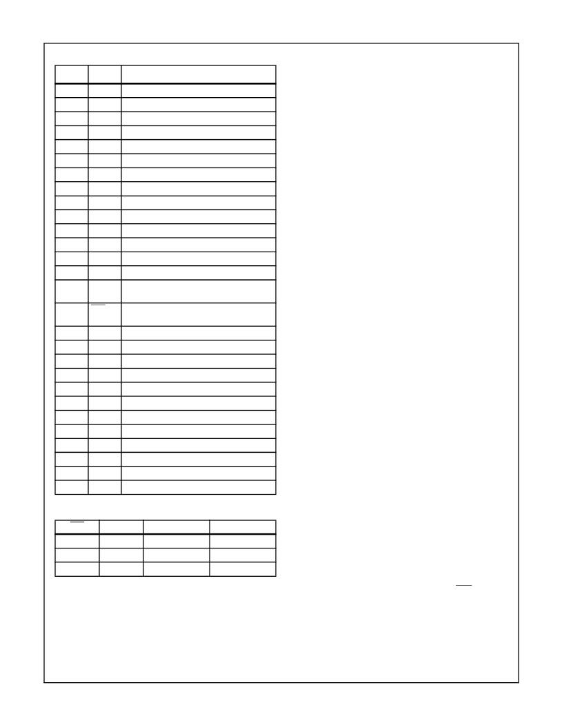
TABLE 1. PIN DESCRIPTION
PIN #
NAME
DESCRIPTION
1
CLK
Clock Input
2
D7
Bit 7, Output (MSB)
3
D6
Bit 6, Output
4
D5
Bit 5, Output
5
D4
Bit 4, Output
6
1
/
4
R
1
/
4
th Point of Reference Ladder
7
V
DD
Digital Power Supply
8
GND
Digital Ground
9
3
/
4
R
3
/
4
th Point of Reference Ladder
10
D3
Bit 3, Output
11
D2
Bit 2, Output
12
D1
Bit 1, Output
13
D0
Bit 0, Output (LSB)
14
OVF
Overflow, Output
15
CE2
Three-State Output Enable Input, Active High.
(See Table 2)
16
CE1
Three-State Output Enable Input, Active Low.
(See Table 2)
17
V
REF
+
Reference Voltage Positive Input
18
AV
DD
Analog Power Supply, +5V
19
AGND
Analog Ground
20
AGND
Analog Ground
21
AV
DD
1
/
2
R
Analog Power Supply, +5V
22
1
/
2
Point of Reference Ladder
23
AV
DD
Analog Power Supply, +5V
24
AGND
Analog Ground
25
AGND
Analog Ground
26
AV
DD
Analog Power Supply, +5V
27
V
REF
-
Reference Voltage Negative Input
28
V
IN
Analog Input
TABLE 2. CHIP ENABLE TRUTH TABLE
CE1
CE2
D0
-
D7
OVF
0
1
Valid
Valid
1
1
Three-State
Valid
X
0
Three-State
Three-State
X’s = Don’t Care.
相关PDF资料 |
PDF描述 |
|---|---|
| HI9P5700J-5 | 8-Bit, 20 MSPS Flash A/D Converter |
| HIF_IOCTL | Using Slow Peripherals with 29K Family Processors Using the HIF ioctl Service for Nonblocking Reads |
| HIF_SPEC | EZ-030 Demonstration Board Theory of Operation Host Interface (HIF) Specification |
| HIGHCURRENTSWITCHINGAPPLICATION | (286.88 k) |
| DC-DCCONVERTERANDMOTORDRIVEAPPLICATIONS | (286.88 k) |
相关代理商/技术参数 |
参数描述 |
|---|---|
| HI3-5701B-9 | 制造商:INTERSIL 制造商全称:Intersil Corporation 功能描述:6-Bit, 30MSPS, Flash A/D Converter |
| HI3-5701K-5 | 制造商:Rochester Electronics LLC 功能描述:- Bulk |
| HI3-574AJN-5 | 功能描述:IC ADC 12BIT 40KSPS 28-PDIP RoHS:否 类别:集成电路 (IC) >> 数据采集 - 模数转换器 系列:- 产品培训模块:Lead (SnPb) Finish for COTS Obsolescence Mitigation Program 标准包装:2,500 系列:- 位数:12 采样率(每秒):3M 数据接口:- 转换器数目:- 功率耗散(最大):- 电压电源:- 工作温度:- 安装类型:表面贴装 封装/外壳:SOT-23-6 供应商设备封装:SOT-23-6 包装:带卷 (TR) 输入数目和类型:- |
| HI3-574AJN-5Z | 功能描述:模数转换器 - ADC W/ANNEAL ADC 12BIT 5 0KSPS COM RoHS:否 制造商:Texas Instruments 通道数量:2 结构:Sigma-Delta 转换速率:125 SPs to 8 KSPs 分辨率:24 bit 输入类型:Differential 信噪比:107 dB 接口类型:SPI 工作电源电压:1.7 V to 3.6 V, 2.7 V to 5.25 V 最大工作温度:+ 85 C 安装风格:SMD/SMT 封装 / 箱体:VQFN-32 |
| HI3-574AKN-5 | 功能描述:IC ADC 12BIT 40KSPS 28-PDIP RoHS:否 类别:集成电路 (IC) >> 数据采集 - 模数转换器 系列:- 产品培训模块:Lead (SnPb) Finish for COTS Obsolescence Mitigation Program 标准包装:2,500 系列:- 位数:12 采样率(每秒):3M 数据接口:- 转换器数目:- 功率耗散(最大):- 电压电源:- 工作温度:- 安装类型:表面贴装 封装/外壳:SOT-23-6 供应商设备封装:SOT-23-6 包装:带卷 (TR) 输入数目和类型:- |
发布紧急采购,3分钟左右您将得到回复。