参数资料
| 型号: | HI5767/6CB |
| 厂商: | Intersil |
| 文件页数: | 5/15页 |
| 文件大小: | 0K |
| 描述: | CONV A/D 10BIT 60MSPS 28-SOIC |
| 标准包装: | 26 |
| 位数: | 10 |
| 采样率(每秒): | 60M |
| 数据接口: | 并联 |
| 转换器数目: | 8 |
| 功率耗散(最大): | 310mW |
| 电压电源: | 模拟和数字 |
| 工作温度: | 0°C ~ 70°C |
| 安装类型: | 表面贴装 |
| 封装/外壳: | 28-SOIC(0.295",7.50mm 宽) |
| 供应商设备封装: | 28-SOIC W |
| 包装: | 管件 |
| 输入数目和类型: | 2 个单端,单极;1 个差分,双极 |
13
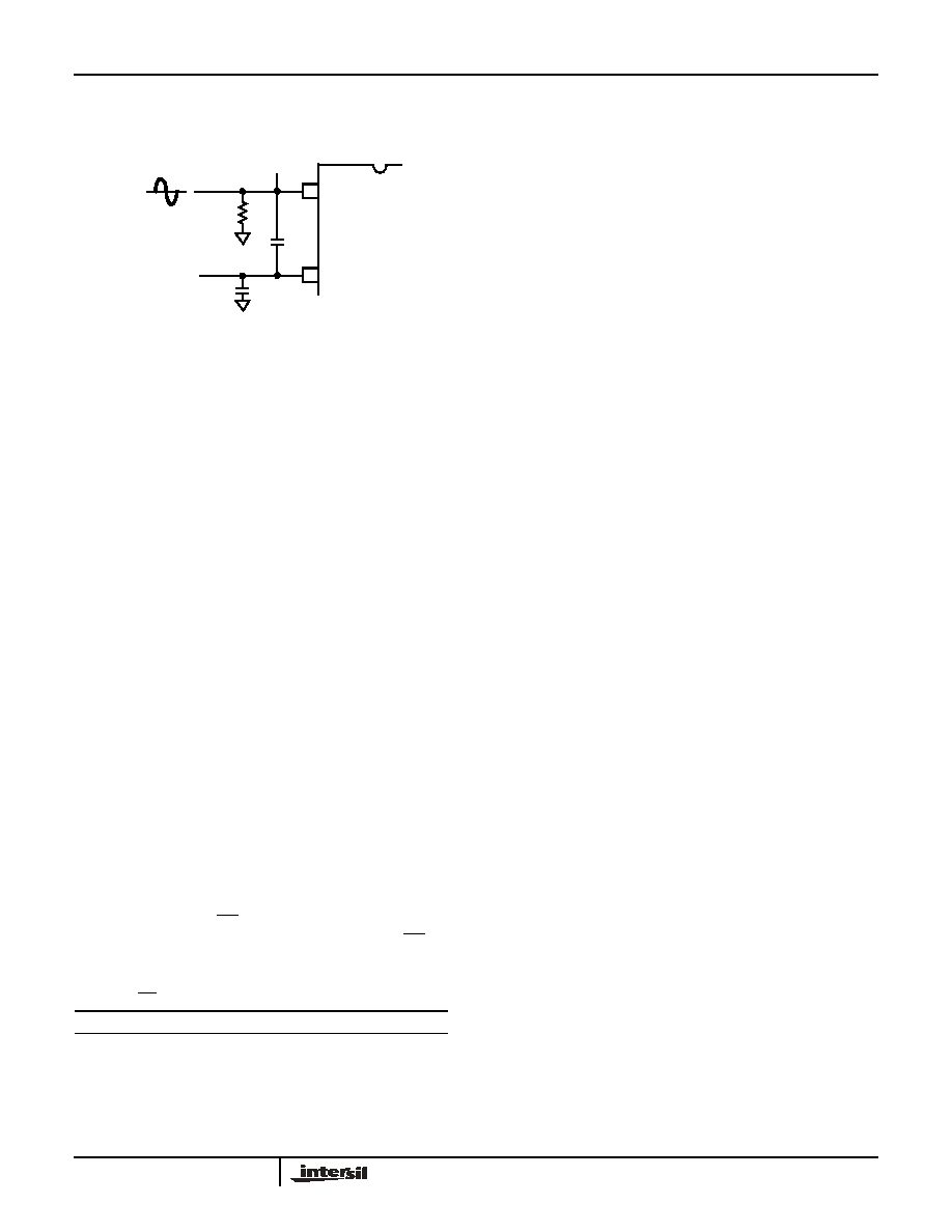
The single ended analog input can be DC coupled
(Figure 20) as long as the input is within the analog input
common mode voltage range.
The resistor, R, in Figure 20 is not absolutely necessary but
may be used as a load setting resistor. A capacitor, C,
connected from VIN+ to VIN- will help filter any high
frequency noise on the inputs, also improving performance.
Values around 20pF are sufficient and can be used on AC
coupled inputs as well. Note, however, that the value of
capacitor C chosen must take into account the highest
frequency component of the analog input signal.
A single ended source may give better overall system
performance if it is first converted to differential before
driving the HI5767.
Digital Output Control and Clock Requirements
The HI5767 provides a standard high-speed interface to
external TTL logic families.
In order to ensure rated performance of the HI5767, the duty
cycle of the clock should be held at 50%
±5%. It must also
have low jitter and operate at standard TTL levels.
Performance of the HI5767 will only be guaranteed at
conversion rates above 1 MSPS. This ensures proper
performance of the internal dynamic circuits. Similarly, when
power is first applied to the converter, a maximum of 20
cycles at a sample rate above 1 MSPS will have to be
performed before valid data is available.A Data Format
Select (DFS) pin is provided which will determine the format
of the digital data outputs. When at logic low, the data will be
output in offset binary format. When at logic high, the data
will be output in two’s complement format. Refer to Table 1
for further information.
The output enable pin, OE, when pulled high will three-state
the digital outputs to a high impedance state. Set the OE
input to logic low for normal operation.
Supply and Ground Considerations
The HI5767 has separate analog and digital supply and
ground pins to keep digital noise out of the analog signal
path. The digital data outputs also have a separate supply
pin, DVCC2 , which can be powered from a 3.0V or 5.0V
supply. This allows the outputs to interface with 3.0V logic if
so desired.
The part should be mounted on a board that provides separate
low impedance connections for the analog and digital supplies
and grounds. For best performance, the supplies to the HI5767
should be driven by clean, linear regulated supplies. The board
should also have good high frequency decoupling capacitors
mounted as close as possible to the converter. If the part is
powered off a single supply, then the analog supply should be
isolated with a ferrite bead from the digital supply.
Refer to the application note “Using Intersil High Speed A/D
Converters” (AN9214) for additional considerations when
using high speed converters.
Static Performance Definitions
Offset Error (VOS)
The midscale code transition should occur at a level 1/4 LSB
above half-scale. Offset is defined as the deviation of the
actual code transition from this point.
Full-Scale Error (FSE)
The last code transition should occur for an analog input that
is 3/4 LSB below Positive Full Scale (+FS) with the offset
error removed. Full scale error is defined as the deviation of
the actual code transition from this point.
Differential Linearity Error (DNL)
DNL is the worst case deviation of a code width from the
ideal value of 1 LSB.
Integral Linearity Error (INL)
INL is the worst case deviation of a code center from a best
fit straight line calculated from the measured data.
Power Supply Sensitivity
Each of the power supplies are moved plus and minus 5% and
the shift in the offset and full scale error (in LSBs) is noted.
Dynamic Performance Definitions
Fast Fourier Transform (FFT) techniques are used to evaluate
the dynamic performance of the HI5767. A low distortion sine
wave is applied to the input, it is coherently sampled, and the
output is stored in RAM. The data is then transformed into the
frequency domain with an FFT and analyzed to evaluate the
dynamic performance of the A/D. The sine wave input to the
part is typically -0.5dB down from full scale for all these tests.
SNR and SINAD are quoted in dB. The distortion numbers are
quoted in dBc (decibels with respect to carrier) and DO NOT
include any correction factors for normalizing to full scale.
The Effective Number of Bits (ENOB) is calculated from the
SINAD data by:
ENOB = (SINAD - 1.76 + VCORR) / 6.02,
OE INPUT
DIGITAL DATA OUTPUTS
0
Active
1
High Impedance
VIN+
VIN-
HI5767
VDC
R
C
VIN
VDC
FIGURE 19. DC COUPLED SINGLE ENDED INPUT
HI5767
相关PDF资料 |
PDF描述 |
|---|---|
| MAX3130EAI+ | IC TXRX W/RS232 28-SSOP |
| MS27484T12F98SA | CONN PLUG 10POS STRAIGHT W/SCKT |
| VI-243-MX-F3 | CONVERTER MOD DC/DC 24V 75W |
| V375C12M150BL3 | CONVERTER MOD DC/DC 12V 150W |
| MS27497P14F35PA | CONN RCPT 37POS WALL MNT W/PINS |
相关代理商/技术参数 |
参数描述 |
|---|---|
| HI5767EVAL1 | 功能描述:数据转换 IC 开发工具 HI5767 LW FREQUENCY EVALUATION PLATFORM RoHS:否 制造商:Texas Instruments 产品:Demonstration Kits 类型:ADC 工具用于评估:ADS130E08 接口类型:SPI 工作电源电压:- 6 V to + 6 V |
| HI5767EVAL2 | 功能描述:数据转换 IC 开发工具 HI5767 HI FREQUENCY EVALUATION PLATFORM RoHS:否 制造商:Texas Instruments 产品:Demonstration Kits 类型:ADC 工具用于评估:ADS130E08 接口类型:SPI 工作电源电压:- 6 V to + 6 V |
| HI5780 | 制造商:INTERSIL 制造商全称:Intersil Corporation 功能描述:10-Bit, 80 MSPS, High Speed, Low Power D/A Converter |
| HI5780-EV | 制造商:INTERSIL 制造商全称:Intersil Corporation 功能描述:10-Bit, 80 MSPS, High Speed, Low Power D/A Converter |
| HI5780JCQ | 制造商:Rochester Electronics LLC 功能描述:32 PQFP COMTEMP VIDEO D/A 10BIT 80MHZ - Bulk 制造商:Harris Corporation 功能描述: |
发布紧急采购,3分钟左右您将得到回复。