参数资料
| 型号: | HI5812JIB |
| 厂商: | Intersil |
| 文件页数: | 2/16页 |
| 文件大小: | 0K |
| 描述: | ADC 12BIT 50KSPS 1.5LSB 24-SOIC |
| 标准包装: | 30 |
| 位数: | 12 |
| 采样率(每秒): | 50k |
| 数据接口: | 并联 |
| 转换器数目: | 1 |
| 功率耗散(最大): | 25mW |
| 电压电源: | 模拟和数字 |
| 工作温度: | -40°C ~ 85°C |
| 安装类型: | 表面贴装 |
| 封装/外壳: | 24-SOIC(0.295",7.50mm 宽) |
| 供应商设备封装: | 24-SOIC |
| 包装: | 管件 |
| 输入数目和类型: | 1 个单端,单极 |
10
Theory of Operation
HI5812 is a CMOS 12-Bit Analog-to-Digital Converter that
uses capacitor-charge balancing to successively approximate
the analog input. A binarily weighted capacitor network forms
the A/D heart of the device. See the block diagram for the
HI5812.
The capacitor network has a common node which is
connected to a comparator. The second terminal of each
capacitor is individually switchable to the input, VREF+ or
VREF-.
During the first three clock periods of a conversion cycle, the
switchable end of every capacitor is connected to the input
and the comparator is being auto-balanced at the capacitor
common node.
During the fourth period, all capacitors are disconnected
from the input; the one representing the MSB (D11) is
connected to the VREF+ terminal; and the remaining
capacitors to VREF-. The capacitor-common node, after the
charges balance out, will indicate whether the input was
above 1/2 of (VREF+ - VREF-). At the end of the fourth
period, the comparator output is stored and the MSB
capacitor is either left connected to VREF+ (if the comparator
was high) or returned to VREF-. This allows the next
comparison to be at either 3/4 or
1/
4 of (VREF+ - VREF -).
At the end of periods 5 through 14, capacitors representing
D10 through D1 are tested, the result stored, and each
capacitor either left at VREF+ or at VREF-.
At the end of the 15th period, when the LSB (D0) capacitor is
tested, (D0) and all the previous results are shifted to the
output registers and drivers. The capacitors are reconnected
to the input, the comparator returns to the balance state, and
the data-ready output goes active. The conversion cycle is
now complete.
Analog Input
The analog input pin is a predominately capacitive load that
changes between the track and hold periods of the
conversion cycle. During hold, clock period 4 through 15, the
input loading is leakage and stray capacitance, typically less
than 5
A and 20pF.
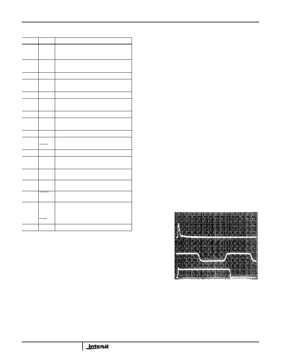
At the start of input tracking, clock period 1, some charge is
dumped back to the input pin. The input source must have
low enough impedance to dissipate the current spike by the
end of the tracking period as shown in Figure 18. The
amount of charge is dependent on supply and input
voltages. The average current is also proportional to clock
frequency.
As long as these current spikes settle completely by end of
the signal acquisition period, converter accuracy will be
preserved. The analog input is tracked for 3 clock cycles.
With an external clock of 750kHz the track period is 4
s.
TABLE 1. PIN DESCRIPTIONS
PIN NO.
NAME
DESCRIPTION
1
DRDY
Output flag signifying new data is available.
Goes high at end of clock period 15. Goes low
when new conversion is started.
2
D0
Bit 0 (Least Significant Bit, LSB).
3
D1
Bit 1.
4
D2
Bit 2.
5
D3
Bit 3.
6
D4
Bit 4.
7
D5
Bit 5.
8
D6
Bit 6.
9
D7
Bit 7.
10
D8
Bit 8.
11
D9
Bit 9.
12
VSS
Digital Ground (0V).
13
D10
Bit 10.
14
D11
Bit 11 (Most Significant Bit, MSB).
15
OEM
Three-State Enable for D4-D11. Active low input.
16
VAA-
Analog Ground, (0V).
17
VAA+
Analog Positive Supply. (+5V) (See text.)
18
VIN
Analog Input.
19
VREF+
Reference Voltage Positive Input, sets 4095
code end of input range.
20
VREF-
Reference Voltage Negative Input, sets 0 code
end of input range.
21
STRT
Start Conversion Input Active Low, recognized
after end of clock period 15.
22
CLK
CLK Input or Output. Conversion functions are
synchronized to positive going edge. (See
text.)
23
OEL
Three-State Enable for D0 D3. Active Low Input.
24
VDD
Digital Positive Supply (+5V).
20mA
10mA
0mA
5V
0V
5V
0V
IIN
CLK
DRDY
200ns/DIV.
CONDITIONS: VDD = VAA+ = 5.0V, VREF+ = 4.608V,
VIN = 4.608V, CLK = 750kHz, TA = 25
oC
FIGURE 18. TYPICAL ANALOG INPUT CURRENT
HI5812
相关PDF资料 |
PDF描述 |
|---|---|
| V375C36M150BL | CONVERTER MOD DC/DC 36V 150W |
| MC100EP116FAR2G | IC TCVR/DRVR HEX DIFF ECL 32LQFP |
| DS2181AQ | IC TXRX CEPT PRIMARY RATE 44PLCC |
| MAX1112EPP+ | IC ADC 8BIT LP 20-DIP |
| NB4N527SMNG | IC DRVR/RCVR/BUFF/XLATOR 16-QFN |
相关代理商/技术参数 |
参数描述 |
|---|---|
| HI5812JIBS2548 | 制造商:Intersil Corporation 功能描述: |
| HI5812JIBZ | 功能描述:ADC 12BIT 50KSPS 1.5LSB 24-SOIC RoHS:是 类别:集成电路 (IC) >> 数据采集 - 模数转换器 系列:- 产品培训模块:Lead (SnPb) Finish for COTS Obsolescence Mitigation Program 标准包装:2,500 系列:- 位数:12 采样率(每秒):3M 数据接口:- 转换器数目:- 功率耗散(最大):- 电压电源:- 工作温度:- 安装类型:表面贴装 封装/外壳:SOT-23-6 供应商设备封装:SOT-23-6 包装:带卷 (TR) 输入数目和类型:- |
| HI5812JIBZ-T | 功能描述:ADC 12BIT SAMPL TRK&HOLD 24-SOIC RoHS:是 类别:集成电路 (IC) >> 数据采集 - 模数转换器 系列:- 产品培训模块:Lead (SnPb) Finish for COTS Obsolescence Mitigation Program 标准包装:2,500 系列:- 位数:12 采样率(每秒):3M 数据接口:- 转换器数目:- 功率耗散(最大):- 电压电源:- 工作温度:- 安装类型:表面贴装 封装/外壳:SOT-23-6 供应商设备封装:SOT-23-6 包装:带卷 (TR) 输入数目和类型:- |
| HI5812JIJ | 制造商:INTERSIL 制造商全称:Intersil Corporation 功能描述:CMOS 20 Microsecond, 12-Bit, Sampling A/D Converter with Internal Track and Hold |
| HI5812JIP | 功能描述:ADC 12BIT 50KSPS 1.5LSB 24-DIP RoHS:否 类别:集成电路 (IC) >> 数据采集 - 模数转换器 系列:- 产品培训模块:Lead (SnPb) Finish for COTS Obsolescence Mitigation Program 标准包装:2,500 系列:- 位数:12 采样率(每秒):3M 数据接口:- 转换器数目:- 功率耗散(最大):- 电压电源:- 工作温度:- 安装类型:表面贴装 封装/外壳:SOT-23-6 供应商设备封装:SOT-23-6 包装:带卷 (TR) 输入数目和类型:- |
发布紧急采购,3分钟左右您将得到回复。