- 您现在的位置:买卖IC网 > PDF目录385381 > HI5905 (Intersil Corporation) 14-Bit, 5 MSPS A/D Converter PDF资料下载
参数资料
| 型号: | HI5905 |
| 厂商: | Intersil Corporation |
| 英文描述: | 14-Bit, 5 MSPS A/D Converter |
| 中文描述: | 14位,5 MSPS的A / D转换 |
| 文件页数: | 7/11页 |
| 文件大小: | 108K |
| 代理商: | HI5905 |
19
Detailed Description
Theory of Operation
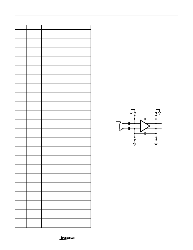
The HI5905 is a 14-bit fully differential sampling pipeline A/D
converter with digital error correction. Figure 8 depicts the
circuit for the front end differential-in-differential-out sample-
and-hold (S/H). The switches are controlled by an internal
clock which is a non-overlapping two phase signal,
φ
1
and
φ
2
, derived from the master clock. During the sampling
phase,
φ
1
, the input signal is applied to the sampling capaci-
tors, C
S
. At the same time the holding capacitors, C
H
, are
discharged to analog ground. At the falling edge of
φ
1
the
input signal is sampled on the bottom plates of the sampling
capacitors. In the next clock phase,
φ
2
, the two bottom
plates of the sampling capacitors are connected together
and the holding capacitors are switched to the op-amp out-
put nodes. The charge then redistributes between C
S
and
C
H
completing one sample-and-hold cycle. The output is a
fully-differential, sampled-data representation of the analog
input. The circuit not only performs the sample-and-hold
function but will also convert a single-ended input to a fully-
differential output for the converter core. During the sampling
phase, the V
IN
pins see only the on-resistance of a switch
and C
S
. The relatively small values of these components
result in a typical full power input bandwidth of 100MHz for
the converter.
As illustrated in the functional block diagram and the timing
diagram in Figure 1, four identical pipeline subconverter stages,
each containing a four-bit flash converter, a four-bit digital-to-
analog converter and an amplifier with a voltage gain of 8,
follow the S/H circuit with the fifth stage being only a 4-bit flash
converter. Each converter stage in the pipeline will be sampling
in one phase and amplifying in the other clock phase. Each
individual sub-converter clock signal is offset by 180 degrees
from the previous stage clock signal, with the result that
alternate stages in the pipeline will perform the same operation.
The output of each of the four-bit subconverter stages is a
four-bit digital word containing a supplementary bit to be used
by the digital error correction logic. The output of each sub-
converter stage is input to a digital delay line which is
controlled by the internal sampling clock. The function of the
digital delay line is to time align the digital outputs of the four
identical four-bit subconverter stages with the corresponding
output of the fifth stage flash converter before applying the
twenty bit result to the digital error correction logic. The digital
error correction logic uses the supplementary bits to correct
any error that may exist before generating the final fourteen bit
digital data output of the converter.
Pin Descriptions
PIN #
NAME
DESCRIPTION
1
NC
No Connection
2
NC
No Connection
3
D
GND1
NC
Digital Ground
4
No Connection
5
AV
CC
A
GND
NC
Analog Supply (5.0V)
6
Analog Ground
7
No Connection
8
NC
No Connection
9
V
IN
+
V
IN
-
V
DC
NC
Positive Analog Input
10
Negative Analog Input
11
DC Bias Voltage Output
12
No Connection
13
V
ROUT
V
RIN
A
GND
AV
CC
NC
Reference Voltage Output
14
Reference Voltage Input
15
Analog Ground
16
Analog Supply (5.0V)
17
No Connection
18
D13
Data Bit 11 Output (MSB)
19
D12
Data Bit 11 Output
20
D11
Data Bit 11 Output
21
D10
Data Bit 10 Output
22
NC
No Connection
23
NC
No Connection
24
D9
Data Bit 9 Output
25
D8
Data Bit 8 Output
26
D
GND2
DV
CC2
NC
Digital Ground
27
Digital Supply (5.0V)
28
No Connection
29
D7
Data Bit 7 Output
30
D6
Data Bit 6 Output
31
D5
Data Bit 5 Output
32
D4
Data Bit 4 Output
33
D3
Data Bit 3 Output
34
NC
No Connection
35
NC
No Connection
36
D2
Data Bit 2 Output
37
D1
Data Bit 1 Output
38
D0
Data Bit 0 Output (LSB)
39
NC
No Connection
40
CLK
Input Clock
41
DV
CC1
D
GND1
DV
CC1
NC
Digital Supply (5.0V)
42
Digital Ground
43
Digital Supply (5.0V)
44
No Connection
C
H
C
S
C
S
V
IN
+
V
OUT
+
V
OUT
-
V
IN
-
φ
1
φ
1
φ
2
φ
1
φ
1
C
H
φ
1
φ
1
+
-
-
+
FIGURE 8. ANALOG INPUT SAMPLE-AND-HOLD
HI5905
相关PDF资料 |
PDF描述 |
|---|---|
| HI5905IN | 14-Bit, 5 MSPS A/D Converter |
| HI5905N | 14-Bit, 5 MSPS, Military A/D Converter |
| HI5905EVAL2 | 14-Bit, 5 MSPS A/D Converter |
| HI7106 | 3 1/2 Digit, LCD/LED Display, A/D Converter |
| HI7106C | 3 1/2 Digit, LCD/LED Display, A/D Converter |
相关代理商/技术参数 |
参数描述 |
|---|---|
| HI5905_03 | 制造商:INTERSIL 制造商全称:Intersil Corporation 功能描述:14-Bit, 5MSPS A/D Converter |
| HI5905BIB | 制造商:未知厂家 制造商全称:未知厂家 功能描述:Converter IC |
| HI5905EVAL2 | 制造商:INTERSIL 制造商全称:Intersil Corporation 功能描述:14-Bit, 5 MSPS, Military A/D Converter |
| HI5905IN | 制造商:Rochester Electronics LLC 功能描述:- Bulk |
| HI5905N | 制造商:INTERSIL 制造商全称:Intersil Corporation 功能描述:14-Bit, 5 MSPS, Military A/D Converter |
发布紧急采购,3分钟左右您将得到回复。