- 您现在的位置:买卖IC网 > PDF目录385381 > HI5905EVAL2 (Intersil Corporation) 14-Bit, 5 MSPS A/D Converter PDF资料下载
参数资料
| 型号: | HI5905EVAL2 |
| 厂商: | Intersil Corporation |
| 英文描述: | 14-Bit, 5 MSPS A/D Converter |
| 中文描述: | 14位,5 MSPS的A / D转换 |
| 文件页数: | 8/11页 |
| 文件大小: | 108K |
| 代理商: | HI5905EVAL2 |
20
Because of the pipeline nature of this converter, the digital
data representing an analog input sample is output to the
digital data bus on the 4th cycle of the clock after the analog
sample is taken. This time delay is specified as the data
latency. After the data latency time, the digital data repre-
senting each succeeding analog sample is output during the
following clock cycle. The digital output data is synchronized
to the external sampling clock with a latch. The digital output
data is available in two’s complement binary format (see
Table 1, A/D Code Table).
Internal Reference Generator, V
ROUT
and V
RIN
The HI5905 has an internal reference generator, therefore,
no external reference voltage is required. V
ROUT
must be
connected to V
RIN
when using the internal reference
voltage.
The HI5905 can be used with an external reference. The
converter requires only one external reference voltage con-
nected to the V
RIN
pin with V
ROUT
left open.
The HI5905 is tested with V
ROUT
, equal to 4.0V, connected
to V
RIN
. Internal to the converter, two reference voltages of
1.3V and 3.3V are generated for a fully differential input
signal range of
±
2V.
In
order
to
minimize
overall
recommended that adequate high frequency decoupling be
provided at the reference voltage input pin, V
RIN
.
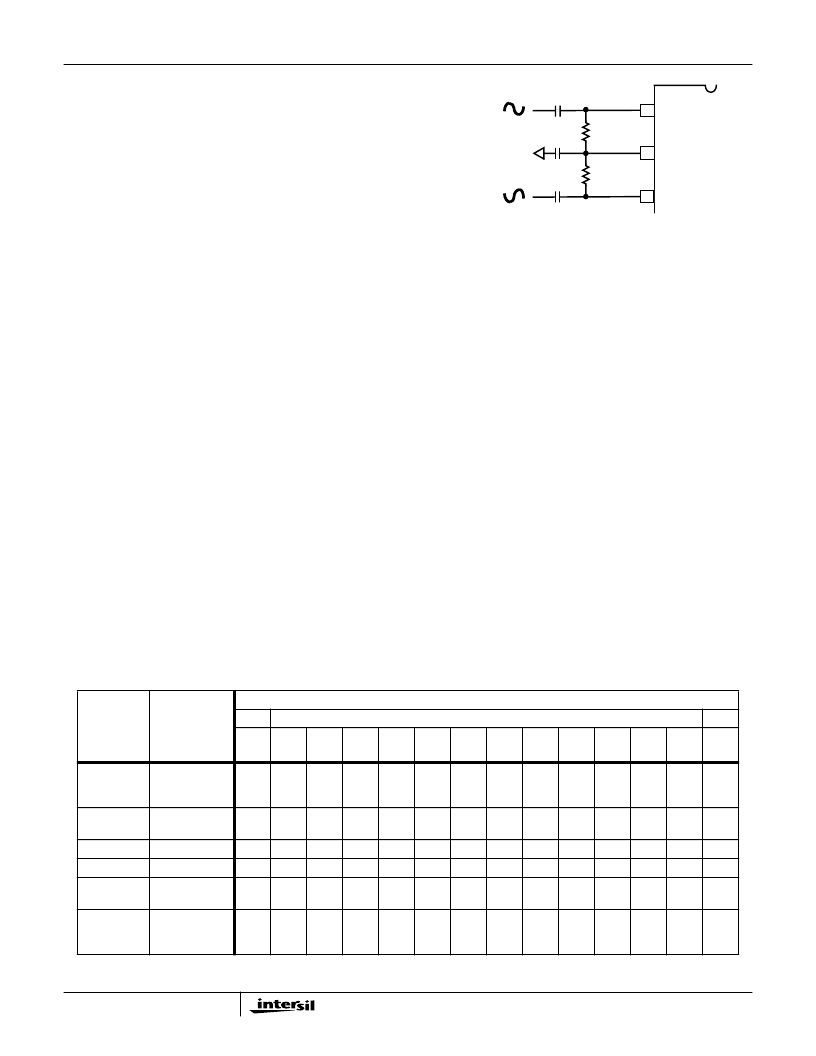
Analog Input, Differential Connection
The analog input to the HI5905 can be configured in various
ways depending on the signal source and the required level
of performance. A fully differential connection (Figure 9) will
give the best performance for the converter.
converter
noise,
it
is
Since the HI5905 is powered off a single +5V supply, the
analog input must be biased so it lies within the analog input
common mode voltage range of 1.0V to 4.0V. The perfor-
mance of the ADC does not change significantly with the
value of the analog input common mode voltage.
A 2.3V DC bias voltage source, V
DC
, half way between the
top and bottom internal reference voltages, is made avail-
able to the user to help simplify circuit design when using a
differential input. This low output impedance voltage source
is not designed to be a reference but makes an excellent
bias source and stays within the analog input common mode
voltage range over temperature.
The difference between the converter’s two internal voltage ref-
erences is 2V. For the AC coupled differential input, (Figure 9), if
V
IN
is a 2V
P-P
sinewave with -V
IN
being 180 degrees out of
phase with V
IN
, then V
IN
+ is a 2V
P-P
sinewave riding on a DC
bias voltage equal to V
DC
and V
IN
- is a 2V
P-P
sinewave riding
on a DC bias voltage equal to V
DC
. Consequently, the con-
verter will be at positive full scale, resulting in a digital data
output code with D13 (MSB) equal to a logic “0” and D0-D12
equal to logic “1” (see Table 1, A/D Code Table), when the V
IN
+
input is at V
DC
+1V and the V
IN
- input is at VDC-1V
(V
IN
+ - V
IN
- = 2V). Conversely, the ADC will be at negative full
scale, resulting in a digital data output code with D13 (MSB)
equal to a logic “1” and D0-D12 equal to logic “0” (see Table 1,
A/D Code Table), when the V
IN
+ input is equal to V
DC
-1V and
V
IN
- is at V
DC
+1V (V
IN
+-V
IN
- = -2V). From this, the converter
is seen to have a peak-to-peak differential analog input voltage
range of 2V
The analog input can be DC coupled (Figure 10) as long as
the inputs are within the analog input common mode voltage
range (1.0V
≤
VDC
≤
4.0V).
V
IN
+
V
DC
V
IN
-
HI5905
V
IN
-
V
IN
FIGURE 9. AC COUPLED DIFFERENTIAL INPUT
TABLE 1. A/D CODE TABLE
CODE
CENTER
DESCRIP-
TION
DIFFERENTIAL
INPUT VOLT-
AGE
€
(USING
INTERNAL
REFERENCE)
TWO’S COMPLEMENT BINARY OUTPUT CODE
MSB
LSB
D13
D12
D11
D10
D9
D8
D7
D6
D5
D4
D3
D2
D1
D0
+Full Scale
(+FS) - 1/4
LSB
+FS
-
1 1/4
LSB
+1.99994V
0
1
1
1
1
1
1
1
1
1
1
1
1
1
1.99969V
0
1
1
1
1
1
1
1
1
1
1
1
1
0
+ 3/4 LSB
183.105
μ
V
-61.035
μ
V
0
0
0
0
0
0
0
0
0
0
0
0
0
0
- 1/4 LSB
1
1
1
1
1
1
1
1
1
1
1
1
1
1
-FS + 1 3/4
LSB
-1.99957V
1
0
0
0
0
0
0
0
0
0
0
0
0
1
-Full Scale
(-FS) + 3/4
LSB
The voltages listed above represent the ideal center of each two’s complement binary output code shown.
-1.99982V
1
0
0
0
0
0
0
0
0
0
0
0
0
0
HI5905
相关PDF资料 |
PDF描述 |
|---|---|
| HI7106 | 3 1/2 Digit, LCD/LED Display, A/D Converter |
| HI7106C | 3 1/2 Digit, LCD/LED Display, A/D Converter |
| HI7106CM44 | 3 1/2 Digit, LCD/LED Display, A/D Converter |
| HI7106CPL | 3 1/2 Digit, LCD/LED Display, A/D Converter |
| HI7106D | 3 1/2 Digit, LCD/LED Display, A/D Converter |
相关代理商/技术参数 |
参数描述 |
|---|---|
| HI5905IN | 制造商:Rochester Electronics LLC 功能描述:- Bulk |
| HI5905N | 制造商:INTERSIL 制造商全称:Intersil Corporation 功能描述:14-Bit, 5 MSPS, Military A/D Converter |
| HI5905N WAF | 制造商:Harris Corporation 功能描述: |
| HI5905N/QML | 制造商:INTERSIL 制造商全称:Intersil Corporation 功能描述:14-Bit, 5 MSPS, Military A/D Converter |
| HI5960 | 制造商:INTERSIL 制造商全称:Intersil Corporation 功能描述:14-Bit, 125+MSPS, CommLinkTM High Speed D/A Converter |
发布紧急采购,3分钟左右您将得到回复。