- 您现在的位置:买卖IC网 > PDF目录385381 > HI7190IB (HARRIS SEMICONDUCTOR) null24-Bit, High Precision, Sigma Delta A/D Converter PDF资料下载
参数资料
| 型号: | HI7190IB |
| 厂商: | HARRIS SEMICONDUCTOR |
| 元件分类: | ADC |
| 英文描述: | null24-Bit, High Precision, Sigma Delta A/D Converter |
| 中文描述: | 1-CH 22-BIT DELTA-SIGMA ADC, SERIAL ACCESS, PDSO20 |
| 文件页数: | 12/24页 |
| 文件大小: | 187K |
| 代理商: | HI7190IB |
1882
verter has an accompanying settling time for step inputs just
as a low pass analog filter does. New data takes between 3
and 4 conversion periods to settle and update on the serial
port with a conversion period t
CONV
being equal to 1/f
N
.
Input Filtering
The digital filter does not provide rejection at integer multi-
ples of the modulator sampling frequency. This implies that
there are frequency bands where noise passes to the output
without attenuation. For most cases this is not a problem
because the high oversampling rate and noise shaping char-
acteristics of the modulator cause this noise to become a
small portion of the broadband noise which is filtered. How-
ever, if an anti-alias filter is necessary a single pole RC filter
is usually sufficient.
If an input filter is used the user must be careful that the
source impedance of the filter is low enough not to cause
gain errors in the system. The DC input impedance at the
inputs is > 1G
but it is a dynamic load that changes with
clock frequency and selected gain. The input sample rate,
also dependent upon clock frequency and gain, determines
the allotted time for the input capacitor to charge. The addi-
tion of external components may cause the charge time of
the capacitor to increase beyond the allotted time. The result
of the input not settling to the proper value is a system gain
error which can be eliminated by system calibration of the
HI7190.
Clocking/Oscillators
The master clock into the HI7190 can be supplied by either a
crystal connected between the OSC
1
and OSC
2
pins as
shown in Figure 11A or a CMOS compatible clock signal
connected to the OSC
1
pin as shown in Figure 11B. The
input sampling frequency, modulator sampling frequency, fil-
ter -3dB frequency, output update rate, and calibration time
are all directly related to the master clock frequency, f
OSC
.
For example, if a 1MHz clock is used instead of a 10MHz
clock, what is normally a 10Hz conversion rate becomes a
1Hz conversion rate. Lowering the clock frequency will also
lower the amount of current drawn from the power supplies.
Please note that the HI7190 specifications are written for a
10MHz clock only.
Operational Modes
The HI7190 contains several operational modes including
calibration modes for cancelling offset and gain errors of
both internal and external circuitry. A calibration routine
should be initiated whenever there is a change in the ambi-
ent operating temperature or supply voltage. Calibration
should also be initiated if there is a change in the gain, filter
notch, bipolar, or unipolar input range. Non-calibrated data
can be obtained from the device by writing 000000 to the
Offset Calibration Register, 800000 (h) to the Positive Full
Scale Calibration Register, and 800000 (h) to the Negative
Full Scale Calibration Register. This sets the offset
correction factor to 0 and both the positive and negative gain
slope factors to 1.
The HI7190 offers several different modes of Self-Calibration
and System Calibration. For calibration to occur, the on-chip
microcontroller must convert the modulator output for three
different input conditions - “zero-scale,” “positive full scale,”
and “negative full scale”. With these readings, the HI7190
can null any offset errors and calculate the gain slope factor
for the transfer function of the converter. It is imperative that
the zero-scale calibration be performed before either of the
gain calibrations. However, the order of the gain calibrations
is not important.
The calibration modes are user selectable in the Control
Register by using the MD bits (MD2-MD0) as shown in
Table 6. DRDY will go low indicating that the calibration is
complete and there is valid data at the output.
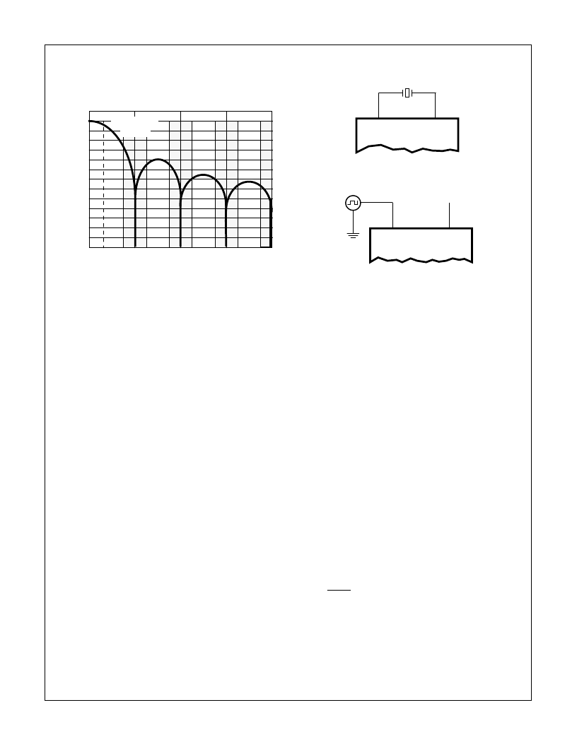
ALIAS BAND
f
N
±
f
C
FREQUENCY (Hz)
A
f
N
f
C
2f
N
3f
N
4f
N
0
-20
-40
-60
-80
-100
-120
FIGURE 9. LOW PASS FILTER FREQUENCY CHARACTERISTICS
FIGURE 10A.
FIGURE 10B.
FIGURE 10. OSCILLATOR CONFIGURATIONS
HI7190
OSC
1
OSC
2
10MHz
16
17
HI7190
OSC
1
OSC
2
10MHz
16
17
NO
CONNECTION
HI7190
相关PDF资料 |
PDF描述 |
|---|---|
| HIH-3602-A | Humidity Sensor(湿度传感器) |
| HIH-3602-L-CP | Humidity Sensor(湿度传感器) |
| HIN240 | 5V High-Speed RS-232 Transceivers with 0.1uF Capacitors |
| HIN240CN | 5V High-Speed RS-232 Transceivers with 0.1uF Capacitors |
| HIP0063 | Potentiometer; Series:CLU; Track Resistance:2.5kohm; Power Rating:2W; Operating Temperature Range:-55 C to +120 C; Adjustment Type:Knob; Leaded Process Compatible:Yes; Mechanical Angle/Rotation:312 RoHS Compliant: Yes |
相关代理商/技术参数 |
参数描述 |
|---|---|
| HI7190IBZ | 功能描述:模数转换器 - ADC ADC 24BIT 10MHZ SIGMADELTA 20 IND RoHS:否 制造商:Texas Instruments 通道数量:2 结构:Sigma-Delta 转换速率:125 SPs to 8 KSPs 分辨率:24 bit 输入类型:Differential 信噪比:107 dB 接口类型:SPI 工作电源电压:1.7 V to 3.6 V, 2.7 V to 5.25 V 最大工作温度:+ 85 C 安装风格:SMD/SMT 封装 / 箱体:VQFN-32 |
| HI7190IBZ-T | 功能描述:模数转换器 - ADC ADC 24BIT 10MHZ SIGMADELTA 20 IND RoHS:否 制造商:Texas Instruments 通道数量:2 结构:Sigma-Delta 转换速率:125 SPs to 8 KSPs 分辨率:24 bit 输入类型:Differential 信噪比:107 dB 接口类型:SPI 工作电源电压:1.7 V to 3.6 V, 2.7 V to 5.25 V 最大工作温度:+ 85 C 安装风格:SMD/SMT 封装 / 箱体:VQFN-32 |
| HI7190IP | 功能描述:IC ADC 24BIT PROGBL SER 20-PDIP RoHS:否 类别:集成电路 (IC) >> 数据采集 - 模数转换器 系列:- 产品培训模块:Lead (SnPb) Finish for COTS Obsolescence Mitigation Program 标准包装:2,500 系列:- 位数:12 采样率(每秒):3M 数据接口:- 转换器数目:- 功率耗散(最大):- 电压电源:- 工作温度:- 安装类型:表面贴装 封装/外壳:SOT-23-6 供应商设备封装:SOT-23-6 包装:带卷 (TR) 输入数目和类型:- |
| HI7190IPZ | 功能描述:模数转换器 - ADC W/ANNEAL ADC 24BIT 1 0HZ SIGMADELTA RoHS:否 制造商:Texas Instruments 通道数量:2 结构:Sigma-Delta 转换速率:125 SPs to 8 KSPs 分辨率:24 bit 输入类型:Differential 信噪比:107 dB 接口类型:SPI 工作电源电压:1.7 V to 3.6 V, 2.7 V to 5.25 V 最大工作温度:+ 85 C 安装风格:SMD/SMT 封装 / 箱体:VQFN-32 |
| HI7191 | 制造商:INTERSIL 制造商全称:Intersil Corporation 功能描述:24-Bit, High Precision, Sigma Delta A/D Converter |
发布紧急采购,3分钟左右您将得到回复。