参数资料
| 型号: | HI7190IBZ-T |
| 厂商: | Intersil |
| 文件页数: | 8/25页 |
| 文件大小: | 0K |
| 描述: | IC ADC 24BIT PROGBL SER 20-SOIC |
| 产品培训模块: | Solutions for Industrial Control Applications |
| 标准包装: | 1,000 |
| 位数: | 24 |
| 数据接口: | 串行,SPI? |
| 转换器数目: | 1 |
| 功率耗散(最大): | 32.5mW |
| 电压电源: | 模拟和数字,双 ± |
| 工作温度: | -40°C ~ 85°C |
| 安装类型: | 表面贴装 |
| 封装/外壳: | 20-SOIC(0.295",7.50mm 宽) |
| 供应商设备封装: | 20-SOIC W |
| 包装: | 带卷 (TR) |
| 输入数目和类型: | 1 个差分,单极;1 个差分,双极 |
16
FN3612.10
June 27, 2006
first SCLK transition output is delayed 29 OSC1 cycles from
the next rising OSC1. SCLK transitions eight times and then
stalls high for 28 OSC1 cycles. After this stall period is
completed SCLK will again transition eight times and stall
high. This sequence will repeat continuously while CS is
active.
The extra OSC1 cycle required when coming out of the CS
inactive state is a one clock cycle latency required to
properly sample the CS input. Note that the normal stall at
byte boundaries is 28 OSC1 cycles thus giving a SCLK rising
to rising edge stall period of 32 OSC1 cycles.
The affects of CS on the I/O are different for self-clocking
mode (MODE = 1) than for external mode (MODE = 0). For
external clocking mode CS inactive disables the I/O state
machine, effectively freezing the state of the I/O cycle. That
is, an I/O cycle can be interrupted using chip select and the
HI7190 will continue with that I/O cycle when re-enabled via
CS. SCLK can continue toggling while CS is inactive. If CS
goes inactive during an I/O cycle, it is up to the user to
ensure that the state of SCLK is identical when reactivating
CS as to what it was when CS went inactive. For read
operations in external clocking mode, the output will go
three-state immediately upon deactivation of CS.
For self-clocking mode (MODE = 1), the affects of CS are
different. If CS transitions high (inactive) during the period
when data is being transferred (any non stall time) the HI7190
will complete the data transfer to the byte boundary. That is,
once SCLK begins the eight transition sequence, it will always
complete the eight cycles. If CS remains inactive after the byte
has been transferred it will be sampled and SCLK will remain
stalled high indefinitely. If CS has returned to active low before
the data byte transfer period is completed the HI7190 acts as
if CS was active during the entire transfer period.
It is important to realize that the user can interrupt a data
transfer on byte boundaries. That is, if the Instruction
Register calls for a 3 byte transfer and CS is inactive after
only one byte has been transferred, the HI7190, when
reactivated, will continue with the remaining two bytes before
looking for the next Instruction Register write cycle.
Note that the outputs will NOT go three-state immediately upon
CS inactive for read operations in self-clocking mode. In the
case of CS going inactive during a read cycle the outputs
remain driving until after the last data bit is transferred. In the
case of CS inactive during the clock stall time it takes 1 OSC1
cycle plus prop delay (Max) for the outputs to be disabled.
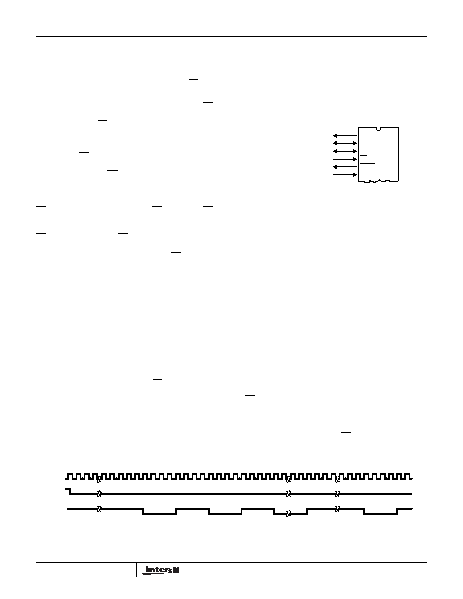
I/O Port Pin Descriptions
The serial I/O port is a bidirectional port which is used to
read the data register and read or write the control register
and calibration registers. The port contains two data lines, a
synchronous clock, and a status flag. Figure 11 shows a
diagram of the serial interface lines.
SDO - Serial Data out. Data is read from this line using those
protocols with separate lines for transmitting and receiving
data. An example of such a standard is the Motorola Serial
Peripheral Interface (SPI) using the 68HC05 and 68HC11
family of microcontrollers, or other similar processors. In the
case of using bidirectional data transfer on SDIO, SDO does
not output data and is set in a high impedance state.
SDIO - Serial Data in or out. Data is always written to the
device on this line. However, this line can be used as a
bidirectional data line. This is done by properly setting up the
Control Register. Bidirectional data transfer on this line can
be used with Intel standard serial interfaces (SSR, Mode 0)
in MCS51 and MCS96 family of microcontrollers, or other
similar processors.
SCLK - Serial clock. The serial clock pin is used to
synchronize data to and from the HI7190 and to run the port
state machines. In Synchronous External Clock Mode, SCLK
is configured as an input, is supplied by the user, and can
run up to a 5MHz rate. In Synchronous Self Clocking Mode,
SCLK is configured as an output and runs at OSC1/8.
CS - Chip select. This signal is an active low input that allows
more than one device on the same serial communication lines.
The SDO and SDIO will go to a high impedance state when this
signal is high. If driven high during any communication cycle,
that cycle will be suspended until CS reactivation. Chip select
can be tied low in systems that maintain control of SCLK.
CHIP SELECT
SDO
SDIO
SCLK
CS
DRDY
HI7190
DEVICE STATUS
BIDIRECTIONAL DATA
DATA OUT
PORT CLOCK
MODE
CLOCK MODE
FIGURE 11. HI7190 SERIAL INTERFACE
OSC1
CS
SCLK
29
33
37
41
45
89
121
125
FIGURE 12. SCLK OUTPUT IN SELF-CLOCKING MODE
HI7190
相关PDF资料 |
PDF描述 |
|---|---|
| VI-B1P-MW-F4 | CONVERTER MOD DC/DC 13.8V 100W |
| GTC030-28-1P | CONN RCPT 9POS PANEL MNT W/PINS |
| VI-B1P-MW-F3 | CONVERTER MOD DC/DC 13.8V 100W |
| MS27508E20F35PA | CONN RCPT 79POS BOX MNT W/PINS |
| ICS1893BFLF | PHYCEIVER LOW PWR 3.3V 48-SSOP |
相关代理商/技术参数 |
参数描述 |
|---|---|
| HI7190IP | 功能描述:IC ADC 24BIT PROGBL SER 20-PDIP RoHS:否 类别:集成电路 (IC) >> 数据采集 - 模数转换器 系列:- 产品培训模块:Lead (SnPb) Finish for COTS Obsolescence Mitigation Program 标准包装:2,500 系列:- 位数:12 采样率(每秒):3M 数据接口:- 转换器数目:- 功率耗散(最大):- 电压电源:- 工作温度:- 安装类型:表面贴装 封装/外壳:SOT-23-6 供应商设备封装:SOT-23-6 包装:带卷 (TR) 输入数目和类型:- |
| HI7190IPZ | 功能描述:模数转换器 - ADC W/ANNEAL ADC 24BIT 1 0HZ SIGMADELTA RoHS:否 制造商:Texas Instruments 通道数量:2 结构:Sigma-Delta 转换速率:125 SPs to 8 KSPs 分辨率:24 bit 输入类型:Differential 信噪比:107 dB 接口类型:SPI 工作电源电压:1.7 V to 3.6 V, 2.7 V to 5.25 V 最大工作温度:+ 85 C 安装风格:SMD/SMT 封装 / 箱体:VQFN-32 |
| HI7191 | 制造商:INTERSIL 制造商全称:Intersil Corporation 功能描述:24-Bit, High Precision, Sigma Delta A/D Converter |
| HI7191_06 | 制造商:INTERSIL 制造商全称:Intersil Corporation 功能描述:24-Bit, High Precision, Sigma Delta A/D Converter |
| HI7191IB | 功能描述:IC ADC 24BIT PROGBL SER 20-SOIC RoHS:否 类别:集成电路 (IC) >> 数据采集 - 模数转换器 系列:- 产品培训模块:Lead (SnPb) Finish for COTS Obsolescence Mitigation Program 标准包装:2,500 系列:- 位数:12 采样率(每秒):3M 数据接口:- 转换器数目:- 功率耗散(最大):- 电压电源:- 工作温度:- 安装类型:表面贴装 封装/外壳:SOT-23-6 供应商设备封装:SOT-23-6 包装:带卷 (TR) 输入数目和类型:- |
发布紧急采购,3分钟左右您将得到回复。