- 您现在的位置:买卖IC网 > PDF目录10589 > HI7191IBZ (Intersil)IC ADC 24BIT PROGBL SER 20-SOIC PDF资料下载
参数资料
| 型号: | HI7191IBZ |
| 厂商: | Intersil |
| 文件页数: | 4/25页 |
| 文件大小: | 0K |
| 描述: | IC ADC 24BIT PROGBL SER 20-SOIC |
| 产品培训模块: | Solutions for Industrial Control Applications |
| 标准包装: | 38 |
| 位数: | 24 |
| 数据接口: | 串行,SPI? |
| 转换器数目: | 1 |
| 功率耗散(最大): | 32.5mW |
| 电压电源: | 模拟和数字,双 ± |
| 工作温度: | -40°C ~ 85°C |
| 安装类型: | 表面贴装 |
| 封装/外壳: | 20-SOIC(0.295",7.50mm 宽) |
| 供应商设备封装: | 20-SOIC W |
| 包装: | 管件 |
| 输入数目和类型: | 1 个差分,单极;1 个差分,双极 |
12
FN4138.8
June 1, 2006
range where the internal operational amplifiers remain in the
linear, high gain region of operation. The HI7191 is designed to
have a range of AVSS +1.8V < VCM < AVDD - 1.8V. Exceeding
this range on the VCM pin will compromise the device
performance.
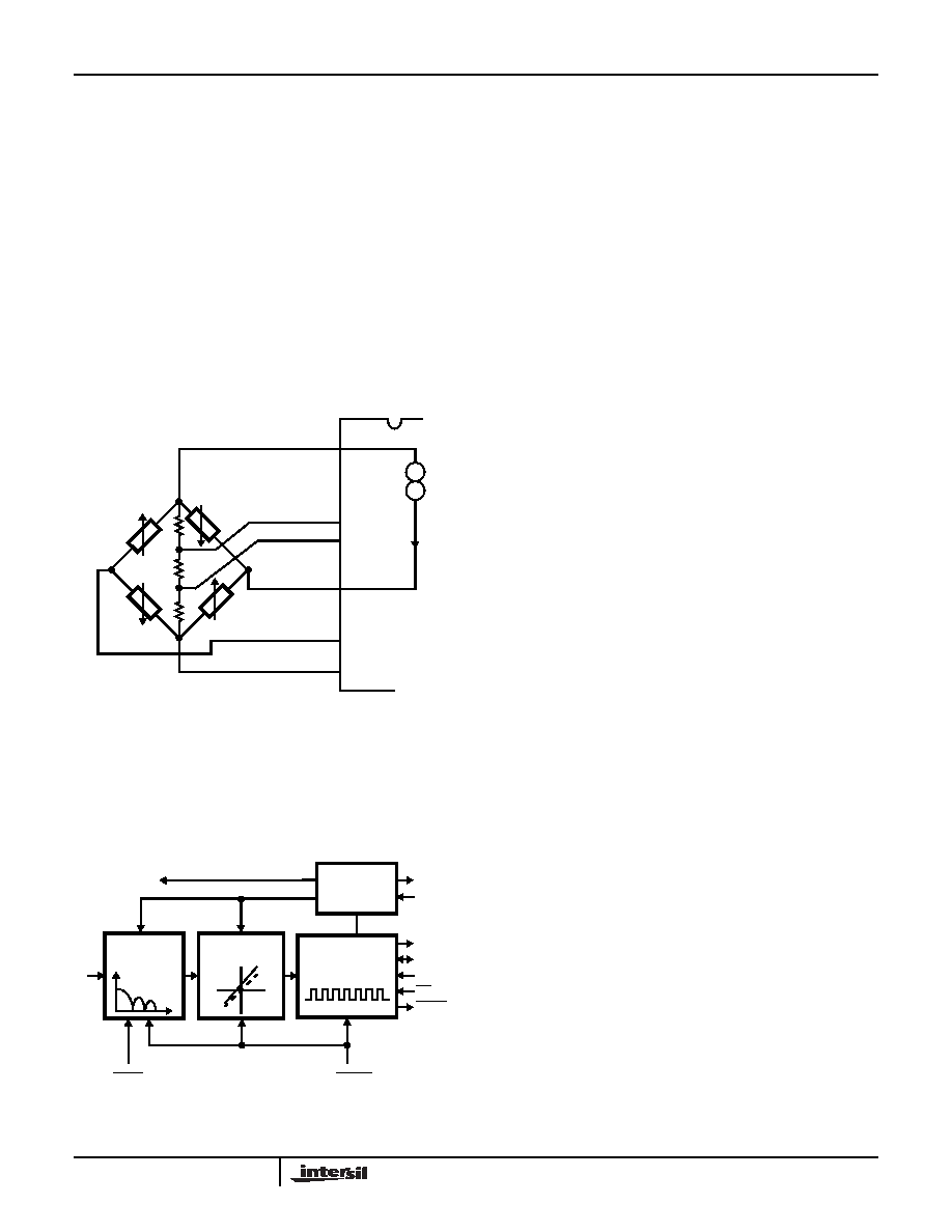
Transducer Burn-Out Current Source
The VINHI input of the HI7191 contains a 500nA (Typ) current
source which can be turned on/off via the Control Register.
This current source can be used in checking whether a
transducer has burnt-out or become open before attempting
to take measurements on that channel. When the current
source is turned on an additional offset will be created
indicating the presence of a transducer. The current source is
controlled by the BO bit (Bit 4) in the Control Register and is
disabled on power up. See Figure 7 for an applications circuit.
Digital Section Description
A block diagram of the digital section of the HI7191 is shown
in Figure 8. This section includes a low pass decimation
filter, conversion controller, calibration logic, serial interface,
and clock generator.
Digital Filtering
One advantage of digital filtering is that it occurs after the
conversion process and can remove noise introduced during
the conversion. It can not, however, remove noise present
on the analog signal prior to the ADC (which an analog filter
can).
One problem with the modulator/digital filter combination is
that excursions outside the full scale range of the device
could cause the modulator and digital filter to saturate. This
device has headroom built in to the modulator and digital
filter which tolerates signal deviations up to 33% outside of
the full scale range of the device. If noise spikes can drive
the input signal outside of this extended range, it is
recommended that an input analog filter is used or the
overall input signal level is reduced.
Low Pass Decimation Filter
The digital low-pass filter is a Hogenauer (sinc3) decimating
filter. This filter was chosen because it is a cost effective low
pass decimating filter that minimizes the need for internal
multipliers and extensive storage and is most effective when
used with high sampling or oversampling rates. Figure 9
shows the frequency characteristics of the filter where fC is
the -3dB frequency of the input signal and fN is the
programmed notch frequency. The analog modulator sends
a one bit data stream to the filter at a rate of that is
determined by:
fMODULATOR = fOSC/128
fMODULATOR = 78.125kHz for fOSC = 10MHz.
The filter then converts the serial modulator data into 40-bit
words for processing by the Hogenauer filter. The data is
decimated in the filter at a rate determined by the CODE
word FP10-FP0 (programed by the user into the Control
Register) and the external clock rate. The equation is:
fNOTCH = fOSC/(512 x CODE).
The Control Register has 11 bits that select the filter cutoff
frequency and the first notch of the filter. The output data
update rate is equal to the notch frequency. The notch
frequency sets the Nyquist sampling rate of the device while
the -3dB point of the filter determines the frequency
spectrum of interest (fS). The FP bits have a usable range of
10 through 2047 where 10 yields a 1.953kHz Nyquist rate.
The Hogenauer filter contains alias components that reflect
around the notch frequency. If the spectrum of the frequency
of interest reaches the alias component, the data has been
aliased and therefore undersampled.
Filter Characteristics
Please note: We have recently discovered a
performance anomaly with the HI7191. The problem
occurs when the digital code for the notch filter is
programmed within certain frequencies. We believe the
error is caused by the calibration logic and the digital
VRHI
VRLO
VINHI
VINLO
AVDD
AVSS
CURRENT
SOURCE
HI7191
RATIOMETRIC
CONFIGURATION
LOAD CELL
FIGURE 7. BURN-OUT CURRENT SOURCE CIRCUIT
MODULATOR
OUTPUT
SERIAL I/O
SDO
SDIO
SCLK
CS
DRDY
RESET
SYNC
OSC2
OSC1
MODULATOR
CLOCK
DIGITAL
CALIBRATION
AND CONTROL
CLOCK
GENERATOR
FILTER
FIGURE 8. DIGITAL SECTION BLOCK DIAGRAM
HI7191
相关PDF资料 |
PDF描述 |
|---|---|
| ISL59885ISZ-T13 | IC SYNC SEPARATOR HD/SD 8-SOIC |
| ISL59885ISZ-T7 | IC VIDEO SYNC SEPARATOR 8-SOIC |
| EL1881CSZ-T7A | IC VIDEO SYNC SEPARATOR 8SOIC |
| HI3-574AKN-5Z | IC ADC 12BIT 40KSPS 28-PDIP |
| PT06A-8-2P | CONN PLUG 2 POS STRAIGHT W/PINS |
相关代理商/技术参数 |
参数描述 |
|---|---|
| HI7191IBZ-T | 功能描述:模数转换器 - ADC ADC 24BIT SIGMADELTA 20 IND RoHS:否 制造商:Texas Instruments 通道数量:2 结构:Sigma-Delta 转换速率:125 SPs to 8 KSPs 分辨率:24 bit 输入类型:Differential 信噪比:107 dB 接口类型:SPI 工作电源电压:1.7 V to 3.6 V, 2.7 V to 5.25 V 最大工作温度:+ 85 C 安装风格:SMD/SMT 封装 / 箱体:VQFN-32 |
| HI7191IP | 功能描述:IC ADC 24BIT PROGBL SER 20-PDIP RoHS:否 类别:集成电路 (IC) >> 数据采集 - 模数转换器 系列:- 产品培训模块:Lead (SnPb) Finish for COTS Obsolescence Mitigation Program 标准包装:2,500 系列:- 位数:12 采样率(每秒):3M 数据接口:- 转换器数目:- 功率耗散(最大):- 电压电源:- 工作温度:- 安装类型:表面贴装 封装/外壳:SOT-23-6 供应商设备封装:SOT-23-6 包装:带卷 (TR) 输入数目和类型:- |
| HI7191IPZ | 功能描述:模数转换器 - ADC W/ANNEAL ADC 24BIT SIGMADELTA 20PDIP RoHS:否 制造商:Texas Instruments 通道数量:2 结构:Sigma-Delta 转换速率:125 SPs to 8 KSPs 分辨率:24 bit 输入类型:Differential 信噪比:107 dB 接口类型:SPI 工作电源电压:1.7 V to 3.6 V, 2.7 V to 5.25 V 最大工作温度:+ 85 C 安装风格:SMD/SMT 封装 / 箱体:VQFN-32 |
| HI73127 | 制造商:Hanna 功能描述:Bulk |
| HI-73127 | 制造商:HANNA INSTRUMENTS 功能描述:ELECTRODE SPARE 制造商:HANNA INSTRUMENTS 功能描述:ELECTRODE, SPARE 制造商:HANNA INSTRUMENTS 功能描述:ELECTRODE, SPARE; pH Measuring Ranges:- |
发布紧急采购,3分钟左右您将得到回复。