- 您现在的位置:买卖IC网 > PDF目录371817 > HIN202ACB-T (HARRIS SEMICONDUCTOR) JT 22C 22#22D PIN WALL RECP PDF资料下载
参数资料
| 型号: | HIN202ACB-T |
| 厂商: | HARRIS SEMICONDUCTOR |
| 元件分类: | 通用总线功能 |
| 英文描述: | JT 22C 22#22D PIN WALL RECP |
| 中文描述: | LINE TRANSCEIVER, PDSO16 |
| 文件页数: | 13/17页 |
| 文件大小: | 247K |
| 代理商: | HIN202ACB-T |
3-13
Detailed Description
The HIN2XXA family of high-speed RS-232
transmitters/receivers are powered by a single +5V power
supply, feature low power consumption, and meet all ElA
RS232C and V.28 specifications. The circuit is divided into
three sections: the charge pump, transmitter, and receiver.
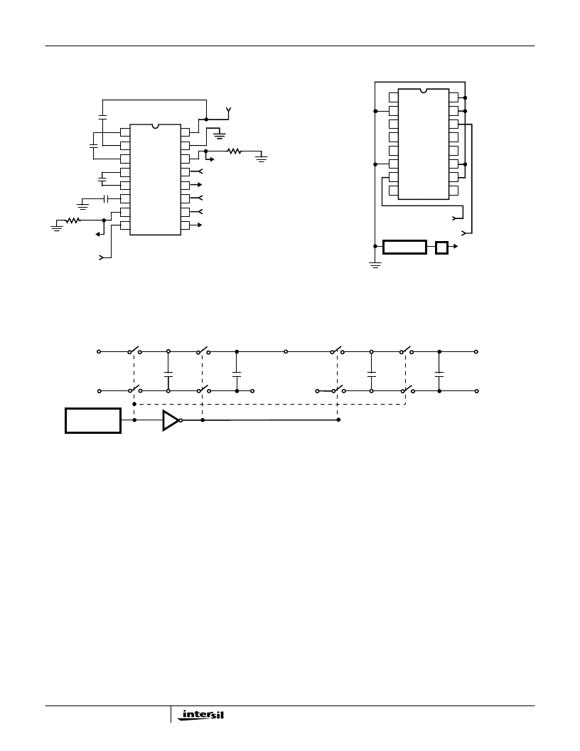
Charge Pump
An equivalent circuit of the charge pump is illustrated in
Figure 3. The charge pump contains two sections: The
voltage doubler and the voltage inverter. Each section is
driven by a two phase, internally generated clock to generate
+10V and -10V. The nominal clock frequency is 125kHz.
During phase one of the clock, capacitor C1 is charged to
V
CC
. During phase two, the voltage on C1 is added to V
CC
,
producing a signal across C3 equal to twice V
CC
. During
phase two, C2 is also charged to 2V
CC
, and then during
phase one, it is inverted with respect to ground to produce a
signal across C4 equal to -2V
CC
. The charge pump accepts
input voltages up to 5.5V. The output impedance of the
voltage doubler section (V+) is approximately 200
, and the
output impedance of the voltage inverter section (V-) is
approximately 450
. A typical application uses 0.1
μ
F
capacitors for C1-C4, however, the value is not critical.
Increasing the values of C1 and C2 will lower the output
impedance of the voltage doubler and inverter, increasing
the values of the reservoir capacitors, C3 and C4, lowers the
ripple on the V+ and V- supplies.
During shutdown mode (HIN205A, HIN206A, HIN211A,
HIN213A, HIN235A, HIN236A and HIN241A, the charge
pump is turned off, V+ is pulled down to V
CC
, V- is pulled up
to GND, and the supply current is reduced to less than 10
μ
A.
The transmitter outputs are disabled and the receiver
outputs (except for HIN213A, R4 and R5) are placed in the
high impedance state.
Test Circuits (HIN232A)
FIGURE 1. GENERAL TEST CIRCUIT
FIGURE 2. POWER-OFF SOURCE RESISTANCE
CONFIGURATION
14
15
16
9
13
12
11
10
1
2
3
4
5
7
6
8
C1+
V+
C1-
C2+
C2-
V-
R2
IN
T2
OUT
V
CC
T1
OUT
R1
IN
R1
OUT
T1
IN
T2
IN
R2
OUT
GND
+4.5V TO
+5.5V INPUT
3k
T1 OUTPUT
RS-232
±
30V INPUT
TTL/CMOS OUTPUT
TTL/CMOS INPUT
TTL/CMOS INPUT
TTL/CMOS OUTPUT
+
-
0.1
μ
F
C3
+
-
0.1
μ
F
C1
+
-
0.1
μ
F
C2
+
-
0.1
μ
F C4
3k
OUTPUT
RS-232
±
30V INPUT
T2
14
15
16
9
13
12
11
10
1
2
3
4
5
7
6
8
C1+
V+
C1-
C2+
C2-
V-
R2
IN
T2
OUT
V
CC
T1
OUT
R1
IN
R1
OUT
T1
IN
T2
IN
R2
OUT
GND
T2
OUT
T1
OUT
V
IN
=
±
2V
A
R
OUT
= V
IN
/I
+
-C1
+
-C3
+
-C2
+
-C4
S1
S2
S5
S6
S3
S4
S7
S8
V
CC
GND
RC
OSCILLATOR
V
CC
GND
V+ = 2V
CC
GND
V- = - (V+)
C1+
C1-
C2-
C2+
VOLTAGE INVERTER
VOLTAGE DOUBLER
FIGURE 3. CHARGE PUMP
HIN202A thru HIN241A
相关PDF资料 |
PDF描述 |
|---|---|
| HIN206ACB-T | JT 22C 22#22D SKT PLUG |
| HIN207ACB-T | JT 22C 22#22D SKT PLUG |
| HIN208ACB-T | JT 22C 22#22D SKT PLUG |
| HIN211ACB-T | JT 22C 22#22D SKT PLUG |
| HIN207IA | PTB 10C 10#20 PIN/SKT RECP |
相关代理商/技术参数 |
参数描述 |
|---|---|
| HIN202ACP | 制造商:Rochester Electronics LLC 功能描述:- Bulk |
| HIN202CA | 制造商:Rochester Electronics LLC 功能描述:16 SSOP,0+70,+5V,2T/2R 0.1 UF CAPS RS-232 - Bulk |
| HIN202CA-T | 制造商:未知厂家 制造商全称:未知厂家 功能描述:Transceiver |
| HIN202CB | 功能描述:IC TXRX RS-232 5V 16-SOIC RoHS:否 类别:集成电路 (IC) >> 接口 - 驱动器,接收器,收发器 系列:- 标准包装:1,000 系列:- 类型:收发器 驱动器/接收器数:2/2 规程:RS232 电源电压:3 V ~ 5.5 V 安装类型:表面贴装 封装/外壳:16-SOIC(0.295",7.50mm 宽) 供应商设备封装:16-SOIC 包装:带卷 (TR) |
| HIN202CBN | 功能描述:IC TXRX RS-232 5V 16-SOIC RoHS:否 类别:集成电路 (IC) >> 接口 - 驱动器,接收器,收发器 系列:- 标准包装:2,500 系列:- 类型:驱动器 驱动器/接收器数:4/0 规程:RS422 电源电压:4.5 V ~ 5.5 V 安装类型:表面贴装 封装/外壳:16-SOIC(0.154",3.90mm 宽) 供应商设备封装:16-SOIC N 包装:带卷 (TR) |
发布紧急采购,3分钟左右您将得到回复。