- 您现在的位置:买卖IC网 > PDF目录371816 > HIN203 (Intersil Corporation) 5V High-Speed RS-232 Transceivers with 0.1uF Capacitors PDF资料下载
参数资料
| 型号: | HIN203 |
| 厂商: | Intersil Corporation |
| 元件分类: | RS-232 |
| 英文描述: | 5V High-Speed RS-232 Transceivers with 0.1uF Capacitors |
| 中文描述: | 5V的高速RS - 232收发器与0.1uF电容 |
| 文件页数: | 11/13页 |
| 文件大小: | 203K |
| 代理商: | HIN203 |
3-11
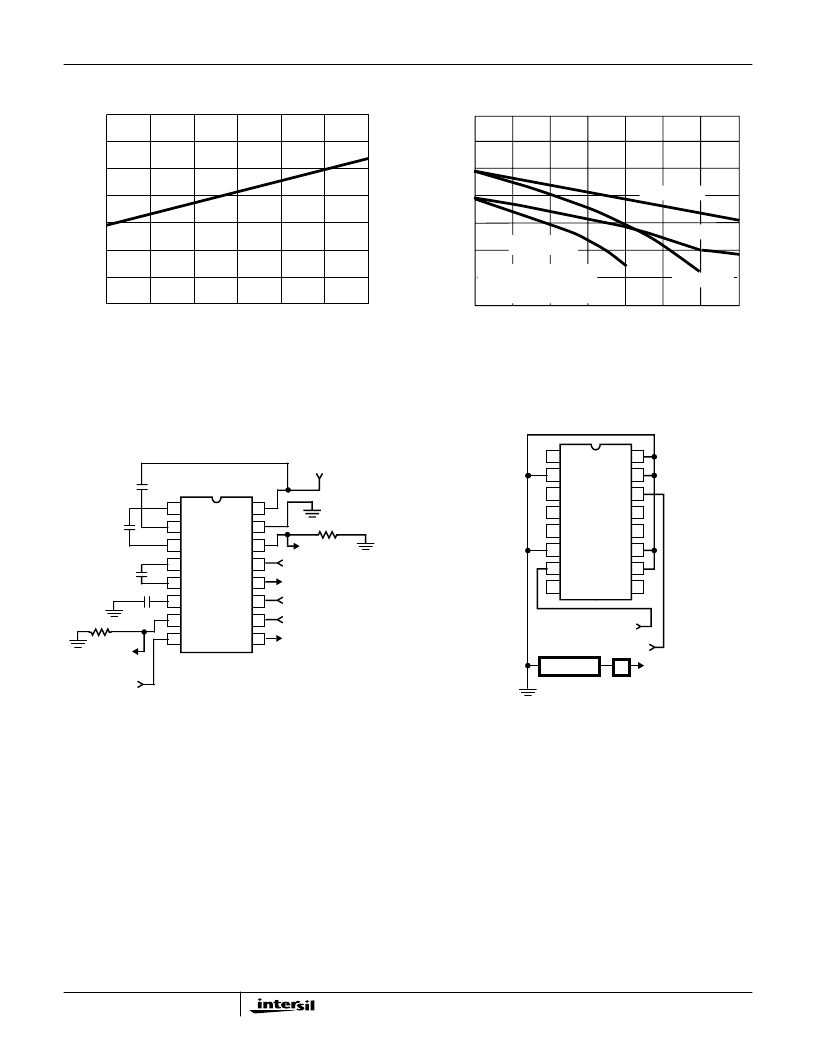
Application Information
The HIN2XX may be used for all RS-232 data terminal and
communication links. It is particularly useful in applications
where
±
12V power supplies are not available for
conventional RS-232 interface circuits. The applications
presented represent typical interface configurations.
A simple duplex RS-232 port with CTS/RTS handshaking is
illustrated in Figure 9. Fixed output signals such as DTR
(data terminal ready) and DSRS (data signaling rate select)
is generated by driving them through a 5kW resistor
connected to V+.
In applications requiring four RS-232 inputs and outputs
(Figure 10), note that each circuit requires two charge pump
capacitors (C1 and C2) but can share common reservoir
capacitors (C3 and C4). The benefit of sharing common
reservoir capacitors is the elimination of two capacitors and
the reduction of the charge pump source impedance which
effectively increases the output swing of the transmitters.
Typical Performance Curves
FIGURE 5.
V- SUPPLY VOLTAGE vs V
CC
FIGURE 6. V+, V- OUTPUT VOLTAGE vs LOAD
12
10
8
6
4
2
0
3.5
4.0
4.5
V
CC
6.0
V
5.0
5.5
3.0
0.1
μ
F
35
|I
LOAD
| (mA)
V+ (V
CC
= 4V)
V+ (V
CC
= 5V)
V- (V
CC
= 5V)
V- (V
CC
= 4V)
T
A
= 25
o
C
TRANSMITTER OUTPUTS
OPEN CIRCUIT
30
25
20
15
10
5
0
S
0
12
10
8
6
4
2
Test Circuits (HIN202)
FIGURE 7. GENERAL TEST CIRCUIT
FIGURE 8. POWER-OFF SOURCE RESISTANCE
CONFIGURATION
14
15
16
9
13
12
11
10
1
2
3
4
5
7
6
8
C1+
V+
C1-
C2+
C2-
V-
R2
IN
T2
OUT
V
CC
T1
OUT
R1
IN
R1
OUT
T1
IN
T2
IN
R2
OUT
GND
+4.5V TO
+5.5V INPUT
3k
T1 OUTPUT
RS-232
±
30V INPUT
TTL/CMOS OUTPUT
TTL/CMOS INPUT
TTL/CMOS INPUT
TTL/CMOS OUTPUT
+
-
0.1
μ
F
C3
+
-
0.1
μ
F
C1
+
-
0.1
μ
F
C2
+
-
0.1
μ
F C4
3k
OUTPUT
RS-232
±
30V INPUT
T2
14
15
16
9
13
12
11
10
1
2
3
4
5
7
6
8
C1+
V+
C1-
C2+
C2-
V-
R2
IN
T2
OUT
V
CC
T1
OUT
R1
IN
R1
OUT
T1
IN
T2
IN
R2
OUT
GND
T2
OUT
T1
OUT
V
IN
=
±
2V
A
R
OUT
= V
IN
/I
HIN201 thru HIN213
相关PDF资料 |
PDF描述 |
|---|---|
| HIN203CB | 5V High-Speed RS-232 Transceivers with 0.1uF Capacitors |
| HIN203CP | 5V High-Speed RS-232 Transceivers with 0.1uF Capacitors |
| HIN205 | 5V High-Speed RS-232 Transceivers with 0.1uF Capacitors |
| HIN205CP | 5V High-Speed RS-232 Transceivers with 0.1uF Capacitors |
| HIN206 | 5V High-Speed RS-232 Transceivers with 0.1uF Capacitors |
相关代理商/技术参数 |
参数描述 |
|---|---|
| HIN203 WAF | 制造商:Harris Corporation 功能描述: |
| HIN203ACB | 制造商:Harris Corporation 功能描述: |
| HIN203ACP | 制造商:Harris Corporation 功能描述: |
| HIN203CB | 制造商:Rochester Electronics LLC 功能描述:20SOIC ,+5V 2D/2R,INTERNAL CAPS,RS-232 - Bulk |
| HIN203CP | 制造商:Rochester Electronics LLC 功能描述:- Bulk |
发布紧急采购,3分钟左右您将得到回复。