- 您现在的位置:买卖IC网 > PDF目录371816 > HIN206IA (INTERSIL CORP) Circular Connector; MIL SPEC:MIL-C-26482, Series I, Crimp; Body Material:Aluminum; Series:PT06; Number of Contacts:16; Connector Shell Size:20; Connecting Termination:Crimp; Circular Shell Style:Straight Plug; Body Style:Straight PDF资料下载
参数资料
| 型号: | HIN206IA |
| 厂商: | INTERSIL CORP |
| 元件分类: | 通用总线功能 |
| 英文描述: | Circular Connector; MIL SPEC:MIL-C-26482, Series I, Crimp; Body Material:Aluminum; Series:PT06; Number of Contacts:16; Connector Shell Size:20; Connecting Termination:Crimp; Circular Shell Style:Straight Plug; Body Style:Straight |
| 中文描述: | LINE TRANSCEIVER, PDSO24 |
| 封装: | SSOP-24 |
| 文件页数: | 10/13页 |
| 文件大小: | 203K |
| 代理商: | HIN206IA |
3-10
Detailed Description
The HIN201 thru HIN213 family of RS-232
transmitters/receivers are powered by a single +5V power
supply (except HIN201), feature low power consumption,
and meet all ElA RS232C and V.28 specifications. The
circuit is divided into three sections: The charge pump,
transmitter, and receiver.
Charge Pump
An equivalent circuit of the charge pump is illustrated in
Figure 1. The charge pump contains two sections: the
voltage doubler and the voltage inverter. Each section is
driven by a two phase, internally generated clock to generate
+10V and -10V. The nominal clock frequency is 125kHz.
During phase one of the clock, capacitor C1 is charged to
V
CC
. During phase two, the voltage on C1 is added to V
CC
,
producing a signal across C3 equal to twice V
CC
. During
phase two, C2 is also charged to 2V
CC
, and then during
phase one, it is inverted with respect to ground to produce a
signal across C4 equal to -2V
CC
. The charge pump accepts
input voltages up to 5.5V. The output impedance of the
voltage doubler section (V+) is approximately 200
, and the
output impedance of the voltage inverter section (V-) is
approximately 450
. A typical application uses 0.1
μ
F
capacitors for C1-C4, however, the value is not critical.
Increasing the values of C1 and C2 will lower the output
impedance of the voltage doubler and inverter, increasing
the values of the reservoir capacitors, C3 and C4, lowers the
ripple on the V+ and V- supplies.
During shutdown mode (HIN205, HIN206 and HIN211,
SD = V
CC
, HIN213, SD = 0V) the charge pump is turned off,
V+ is pulled down to V
CC
, V- is pulled up to GND, and the
supply current is reduced to less than 10
μ
A. The transmitter
outputs are disabled and the receiver outputs (except for
HIN213, R4 and R5) are placed in the high impedance state.
Transmitters
The transmitters are TTL/CMOS compatible inverters which
translate the inputs to RS-232 outputs. The input logic
threshold is about 26% of V
CC
, or 1.3V for V
CC
= 5V. A logic
1 at the input results in a voltage of between -5V and V- at
the output, and a logic 0 results in a voltage between +5V
and (V+ - 0.6V). Each transmitter input has an internal
400k
pullup resistor so any unused input can be left
unconnected and its output remains in its low state. The
output voltage swing meets the RS-232C specifications of
±
5V minimum with the worst case conditions of: all
transmitters driving 3k
minimum load impedance, V
CC
=
4.5V, and maximum allowable operating temperature. The
transmitters have an internally limited output slew rate which
is less than 30V/
μ
s. The outputs are short circuit protected
and can be shorted to ground indefinitely. The powered
down output impedance is a minimum of 300
with
±
2V
applied to the outputs and V
CC
= 0V.
Receivers
The receiver inputs accept up to
±
30V while presenting the
required 3k
to 7k
input impedance even if the power is off
(V
CC
= 0V). The receivers have a typical input threshold of
1.3V which is within the
±
3V limits, known as the transition
region, of the RS-232 specifications. The receiver output is
0V to V
CC
. The output will be low whenever the input is
greater than 2.4V and high whenever the input is floating or
driven between +0.8V and -30V. The receivers feature 0.5V
hysteresis (except during shutdown) to improve noise
rejection. The receiver Enable line (EN, on HIN205, HIN206
and HIN211, EN on HIN213) when unasserted, disables the
receiver outputs, placing them in the high impedance mode.
The receiver outputs are also placed in the high impedance
state when in shutdown mode (except HIN213 R4 and R5).
HIN213 Operation in Shutdown
The HIN213 features two receivers, R4 and R5, which
remain active in shutdown mode. During normal operation
the receivers propagation delay is typically 0.5
μ
s. This
propagation delay may increase slightly during shutdown.
When entering shut down mode, receivers R4 and R5 are
not valid for 80
μ
s after SD = V
IL
. When exiting shutdown
mode, all receiver outputs will be invalid until the charge
pump circuitry reaches normal operating voltage. This is
typically less than 2ms when using 0.1
μ
F capacitors.
T
OUT
V- < V
TOUT
< V+
300
400k
T
XIN
GND < T
XIN
< V
CC
V-
V+
V
CC
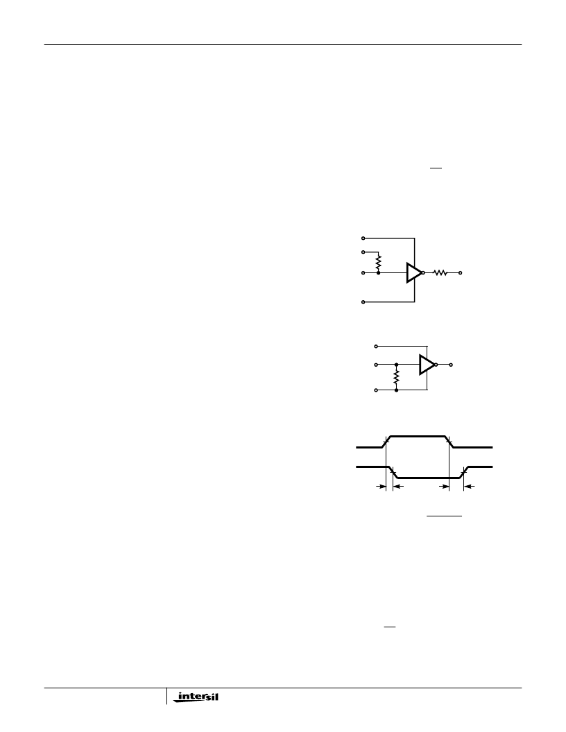
FIGURE 2. TRANSMITTER
R
OUT
GND < V
ROUT
< V
CC
5k
R
XIN
-30V < R
XIN
< +30V
GND
V
CC
FIGURE 3. RECEIVER
T
IN
OR
R
IN
V
OL
V
OL
t
PLH
t
PHL
AVERAGE PROPAGATION DELAY =
t
PHL +
t
PLH
2
T
OUT
OR
R
OUT
FIGURE 4. PROPAGATION DELAY DEFINITION
HIN201 thru HIN213
相关PDF资料 |
PDF描述 |
|---|---|
| HIN206IB | Circular Connector; Body Material:Aluminum; Series:PT06; No. of Contacts:16; Connector Shell Size:20; Connecting Termination:Crimp; Circular Shell Style:Straight Plug; Circular Contact Gender:Socket; Insert Arrangement:20-16 |
| HIN230 | 5V High-Speed RS-232 Transceivers with 0.1uF Capacitors |
| HIN234IB | 5V High-Speed RS-232 Transceivers with 0.1uF Capacitors |
| HIN237IP | 5V High-Speed RS-232 Transceivers with 0.1uF Capacitors |
| HIN237ECA-T | 5V High-Speed RS-232 Transceivers with 0.1uF Capacitors |
相关代理商/技术参数 |
参数描述 |
|---|---|
| HIN206IA-T | 制造商:未知厂家 制造商全称:未知厂家 功能描述:Interface IC |
| HIN206IB | 制造商:Rochester Electronics LLC 功能描述:RS232 5V 4D/3R 0.1UF CAPS 24SOIC IND - Bulk |
| HIN206IP | 制造商:HARRIS 制造商全称:HARRIS 功能描述:+5V Powered RS-232 Transmitters/Receivers with 0.1Microfarad External Capacitors |
| HIN207 | 制造商:未知厂家 制造商全称:未知厂家 功能描述:+5V Powered RS-232 Transmitters/Receivers' with 0.1Microfarad External Capacitors |
| HIN207A | 制造商:INTERSIL 制造商全称:Intersil Corporation 功能描述:High Speed +5V Powered RS-232 Transmitters/Receivers |
发布紧急采购,3分钟左右您将得到回复。