参数资料
| 型号: | HIN207EIBZ-T |
| 厂商: | Intersil |
| 文件页数: | 2/22页 |
| 文件大小: | 0K |
| 描述: | IC 5DRVR/3RCVR RS232 5V 24-SOIC |
| 标准包装: | 1,000 |
| 类型: | 收发器 |
| 驱动器/接收器数: | 5/3 |
| 规程: | RS232 |
| 电源电压: | 4.75 V ~ 5.25 V |
| 安装类型: | 表面贴装 |
| 封装/外壳: | 24-SOIC(0.295",7.50mm 宽) |
| 供应商设备封装: | 24-SOIC |
| 包装: | 带卷 (TR) |
10
FN4315.16
November 4, 2005
Detailed Description
The HIN2XXE family of high-speed RS-232
transmitters/receivers are powered by a single +5V power
supply, feature low power consumption, and meet all ElA
RS232C and V.28 specifications. The circuit is divided into
three sections: the charge pump, transmitter, and receiver.
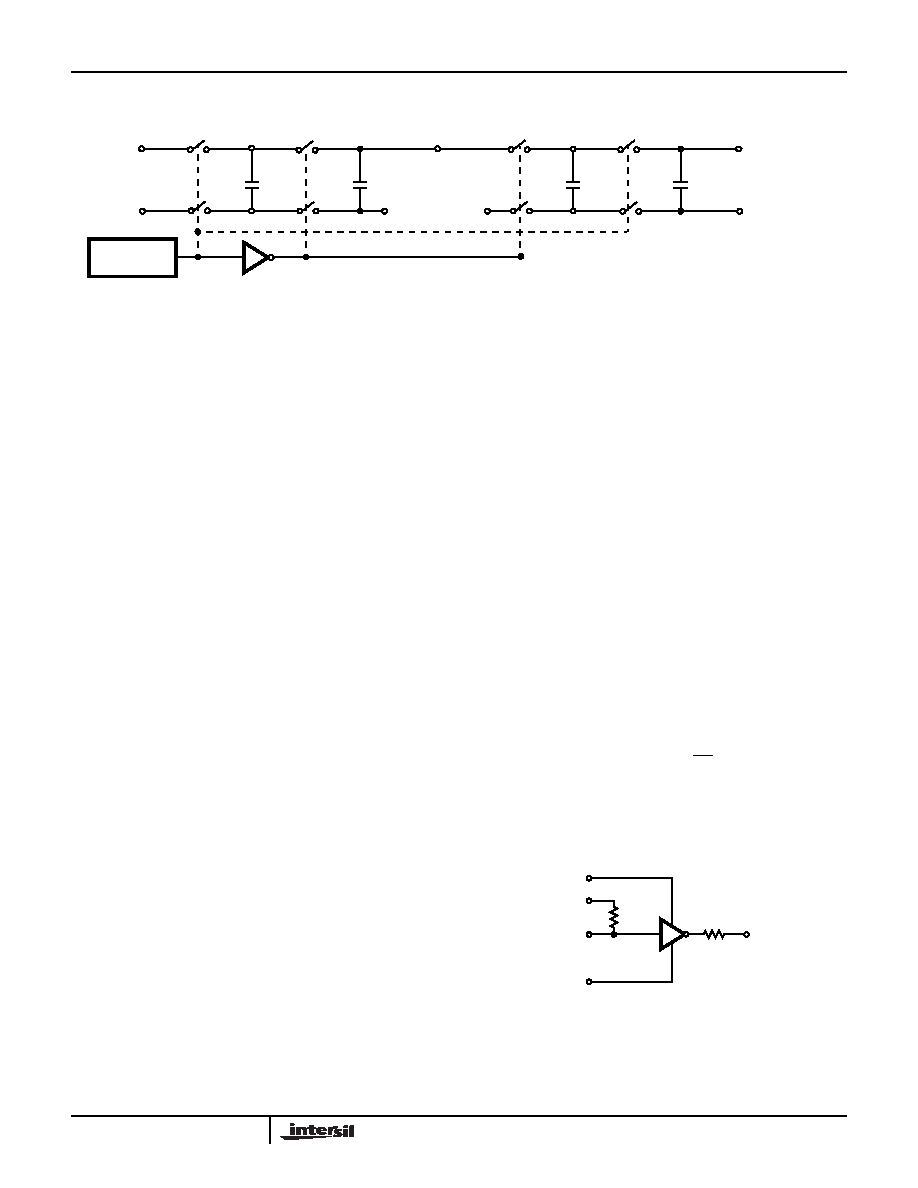
Charge Pump
An equivalent circuit of the charge pump is illustrated in
Figure 3. The charge pump contains two sections: the
voltage doubler and the voltage inverter. Each section is
driven by a two phase, internally generated clock to
generate +10V and -10V. The nominal clock frequency is
125kHz. During phase one of the clock, capacitor C1 is
charged to VCC . During phase two, the voltage on C1 is
added to VCC, producing a signal across C3 equal to twice
VCC. During phase two, C2 is also charged to 2VCC, and
then during phase one, it is inverted with respect to ground
to produce a signal across C4 equal to -2VCC. The charge
pump accepts input voltages up to 5.5V. The output
impedance of the voltage doubler section (V+) is
approximately 200
, and the output impedance of the
voltage inverter section (V-) is approximately 450
. A typical
application uses 0.1
F capacitors for C1-C4, however, the
value is not critical. Increasing the values of C1 and C2 will
lower the output impedance of the voltage doubler and
inverter, increasing the values of the reservoir capacitors, C3
and C4, lowers the ripple on the V+ and V- supplies.
During shutdown mode (HIN206E, HIN211E and HIN213E)
the charge pump is turned off, V+ is pulled down to VCC, V-
is pulled up to GND, and the supply current is reduced to
less than 10
A. The transmitter outputs are disabled and the
receiver outputs (except for HIN213E, R4 and R5) are
placed in the high impedance state.
Transmitters
The transmitters are TTL/CMOS compatible inverters which
translate the inputs to RS-232 outputs. The input logic
threshold is about 26% of VCC, or 1.3V for VCC = 5V. A logic
1 at the input results in a voltage of between -5V and V- at
the output, and a logic 0 results in a voltage between +5V
and (V+ -0.6V). Each transmitter input has an internal 400k
pullup resistor so any unused input can be left unconnected
and its output remains in its low state. The output voltage
swing meets the RS-232C specifications of
±5V minimum
with the worst case conditions of: all transmitters driving 3k
minimum load impedance, VCC = 4.5V, and maximum
allowable operating temperature. The transmitters have an
internally limited output slew rate which is less than 30V/
s.
The outputs are short circuit protected and can be shorted to
ground indefinitely. The powered down output impedance is
a minimum of 300
with ±2V applied to the outputs and
VCC = 0V.
Receivers
The receiver inputs accept up to
±30V while presenting the
required 3k
to 7k input impedance even if the power is off
(VCC = 0V). The receivers have a typical input threshold of
1.3V which is within the
±3V limits, known as the transition
region, of the RS-232 specifications. The receiver output is
0V to VCC. The output will be low whenever the input is
greater than 2.4V and high whenever the input is floating or
driven between +0.8V and -30V. The receivers feature 0.5V
hysteresis (except during shutdown) to improve noise
rejection. The receiver Enable line EN, (EN on HIN213E)
when unasserted, disables the receiver outputs, placing
them in the high impedance mode. The receiver outputs are
also placed in the high impedance state when in shutdown
mode (except HIN213E R4 and R5).
+
-
C1
+
-
C3
+
-
C2
+
-
C4
S1
S2
S5
S6
S3
S4
S7
S8
VCC
GND
RC
OSCILLATOR
VCC
GND
V+ = 2VCC
GND
V
- = - (V+)
C1+
C1
-
C2
-
C2+
VOLTAGE INVERTER
VOLTAGE DOUBLER
FIGURE 3. CHARGE PUMP
TOUT
V- < VTOUT < V+
300
400k
TXIN
GND < TXIN < VCC
V-
V+
VCC
FIGURE 4. TRANSMITTER
HIN202E, HIN206E, HIN207E, HIN208E, HIN211E, HIN213E, HIN232E
相关PDF资料 |
PDF描述 |
|---|---|
| VE-BWN-MW-F3 | CONVERTER MOD DC/DC 18.5V 100W |
| MS3106E22-14SY | CONN PLUG 19POS STRAIGHT W/SCKT |
| MS27499E10B13SA | CONN RCPT 13POS BOX MNT W/SCKT |
| MAX1241CCPA+ | IC ADC 12BIT SERIAL 8-DIP |
| MAX1262BCEI+ | IC ADC 12BIT 400KSPS 28-QSOP |
相关代理商/技术参数 |
参数描述 |
|---|---|
| HIN207EIP | 制造商:Rochester Electronics LLC 功能描述:24LEAD PDIP 15KV PROTECTED RS-232 SERIAL IND - Bulk |
| HIN207IA | 制造商:Rochester Electronics LLC 功能描述:- Bulk |
| HIN207IA-T | 制造商:未知厂家 制造商全称:未知厂家 功能描述:Interface IC |
| HIN207IB | 制造商:Rochester Electronics LLC 功能描述:RS232 5V 5D/3R 24SOIC IND - Bulk |
| HIN207IP | 制造商:Rochester Electronics LLC 功能描述:- Bulk |
发布紧急采购,3分钟左右您将得到回复。