参数资料
| 型号: | HIN237CBZ-T |
| 厂商: | Intersil |
| 文件页数: | 2/21页 |
| 文件大小: | 0K |
| 描述: | IC 5DRVR/3RCVR RS232 5V 24-SOIC |
| 标准包装: | 1,000 |
| 类型: | 收发器 |
| 驱动器/接收器数: | 5/3 |
| 规程: | RS232 |
| 电源电压: | 4.5 V ~ 5.5 V |
| 安装类型: | 表面贴装 |
| 封装/外壳: | 24-SOIC(0.295",7.50mm 宽) |
| 供应商设备封装: | 24-SOIC |
| 包装: | 带卷 (TR) |
10
FN3138.16
September 26, 2008
Detailed Description
The HIN232 thru HIN241 family of RS-232
transmitters/receivers are powered by a single +5V power
supply (except HIN239), feature low power consumption, and
meet all ElA RS-232C and V.28 specifications. The circuit is
divided into three sections: The charge pump, transmitter, and
receiver.
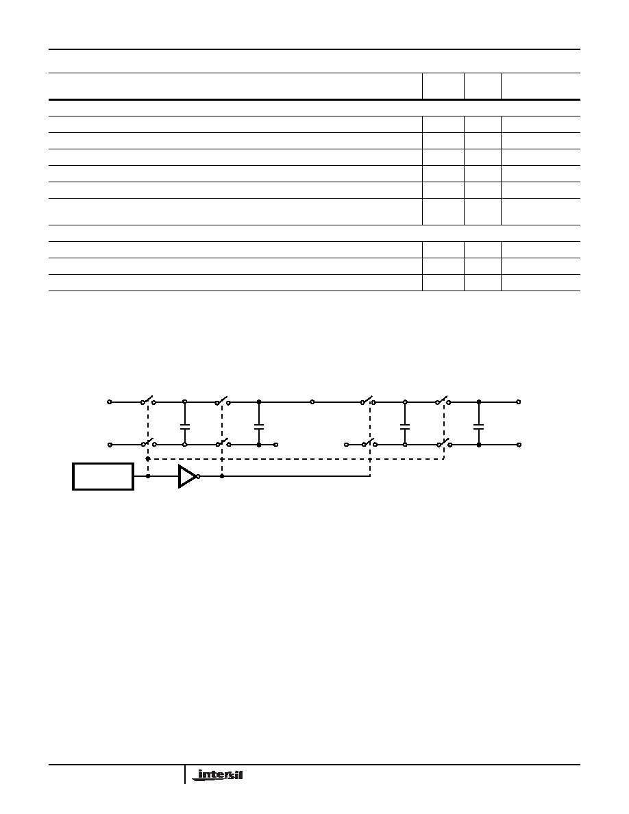
Charge Pump
An equivalent circuit of the charge pump is illustrated in
Figure 1. The charge pump contains two sections: the voltage
doubler and the voltage inverter. Each section is driven by a
two-phase, internally generated clock to generate +10V and
-10V. The nominal clock frequency is 16kHz. During phase
one of the clock, capacitor C1 is charged to VCC. During
phase two, the voltage on C1 is added to VCC, producing a
signal across C3 equal to twice VCC. During phase one, C2 is
also charged to 2VCC, and then during phase two, it is
inverted with respect to ground to produce a signal across C4
equal to -2VCC. The charge pump accepts input voltages up
to 5.5V. The output impedance of the voltage doubler section
(V+) is approximately 200
Ω, and the output impedance of the
voltage inverter section (V-) is approximately 450
Ω. A typical
application uses 1F capacitors for C1-C4, however, the value
is not critical. Increasing the values of C1 and C2 will lower the
output impedance of the voltage doubler and inverter,
increasing the values of the reservoir capacitors, C3 and C4,
lowers the ripple on the V+ and V- supplies.
During shutdown mode (HIN236, HIN240 and HIN241),
SHUTDOWN control line set to logic “1”, the charge pump is
turned off, V+ is pulled down to VCC, V- is pulled up to GND,
and the supply current is reduced to less than 10A. The
transmitter outputs are disabled and the receiver outputs are
placed in the high impedance state.
TIMING CHARACTERISTICS
Baud Rate (1 Transmitter Switching)
RL = 3kΩ
120
-
kbps
Output Enable Time, tEN
HIN236, HIN239, HIN240, HIN241
-
400
-
ns
Output Disable Time, tDIS
HIN236, HIN239, HIN240, HIN241
-
250
-
ns
Propagation Delay, tPD
RS-232 to TTL
-
0.5
-
s
Instantaneous Slew Rate SR
-
30
V/s
Transition Region Slew Rate, SRT
RL = 3kΩ, CL = 2500pF Measured from +3V to -3V
or -3V to +3V, 1 Transmitter Switching
-3
-
V/s
TRANSMITTER OUTPUTS
Output Voltage Swing, TOUT
Transmitter Outputs, 3k
Ω to Ground
±5
±9
±10
V
Output Resistance, TOUT
VCC = V+ = V- = 0V, VOUT = ±2V
300
-
Ω
RS-232 Output Short Circuit Current, ISC
TOUT shorted to GND
-
±10
-
mA
NOTE:
4. Limits established by characterization and are not production tested.
5. Parameters with MIN and/or MAX limits are 100% tested at +25°C, unless otherwise specified. Temperature limits established by characterization
and are not production tested.
Electrical Specifications
Test Conditions: VCC = +5V ±10%, TA = Operating Temperature Range (Continued)
PARAMETER
TEST CONDITIONS
MIN
(Note 5)
TYP
MAX
(Note 5)
UNITS
+
-
C1
+
-
C3
+
-
C2
+
-
C4
S1
S2
S5
S6
S3
S4
S7
S8
VCC
GND
RC
OSCILLATOR
VCC
GND
V+ = 2VCC
GND
V- = -(V+)
C1+
C1-
C2-
C2+
VOLTAGE INVERTER
VOLTAGE DOUBLER
FIGURE 1. CHARGE PUMP
HIN232, HIN236, HIN237, HIN238, HIN239, HIN240, HIN241
相关PDF资料 |
PDF描述 |
|---|---|
| MAX157BEPA+ | IC ADC 10BIT 108KSPS 2CH 8-DIP |
| IDT72V285L15TF | IC FIFO SS 65536X18 15NS 64STQFP |
| HIN237CBZ | IC 5DRVR/3RCVR RS232 5V 24-SOIC |
| MAX157ACPA+ | IC ADC 10BIT 108KSPS 2CH 8-DIP |
| VI-BW1-MW-F2 | CONVERTER MOD DC/DC 12V 100W |
相关代理商/技术参数 |
参数描述 |
|---|---|
| HIN237CP | 制造商:Rochester Electronics LLC 功能描述:- Bulk 制造商:Harris Corporation 功能描述: |
| HIN237E | 制造商:INTERSIL 制造商全称:Intersil Corporation 功能描述:+/-15kV, ESD-Protected, +5V Powered,RS-232 Transmitters/Receivers |
| HIN237ECA | 制造商:Rochester Electronics LLC 功能描述:- Bulk |
| HIN237ECA-T | 制造商:INTERSIL 制造商全称:Intersil Corporation 功能描述:+/-15kV, ESD-Protected, +5V Powered,RS-232 Transmitters/Receivers |
| HIN237ECB | 制造商:Rochester Electronics LLC 功能描述:- Bulk |
发布紧急采购,3分钟左右您将得到回复。