- 您现在的位置:买卖IC网 > PDF目录299176 > HIN238ECB-T (INTERSIL CORP) QUAD LINE TRANSCEIVER, PDSO24 PDF资料下载
参数资料
| 型号: | HIN238ECB-T |
| 厂商: | INTERSIL CORP |
| 元件分类: | Line Driver or Receiver |
| 英文描述: | QUAD LINE TRANSCEIVER, PDSO24 |
| 封装: | PLASTIC, MS-013AD, SOIC-24 |
| 文件页数: | 3/23页 |
| 文件大小: | 316K |
| 代理商: | HIN238ECB-T |
11
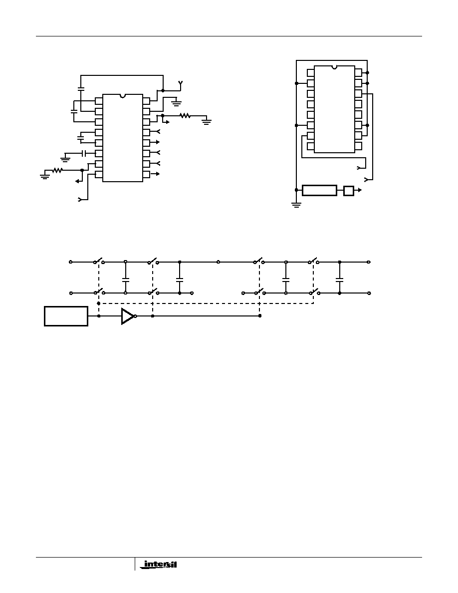
Detailed Description
The HIN2XXE family of high-speed RS-232
transmitters/receivers are powered by a single +5V power
supply, feature low power consumption, and meet all ElA
RS232C and V.28 specications. The circuit is divided into
three sections: the charge pump, transmitter, and receiver.
Charge Pump
An equivalent circuit of the charge pump is illustrated in
Figure 3. The charge pump contains two sections: the
voltage doubler and the voltage inverter. Each section is
driven by a two phase, internally generated clock to generate
+10V and -10V. The nominal clock frequency is 125kHz.
During phase one of the clock, capacitor C1 is charged to
VCC . During phase two, the voltage on C1 is added to VCC,
producing a signal across C3 equal to twice VCC. During
phase two, C2 is also charged to 2VCC, and then during
phase one, it is inverted with respect to ground to produce a
signal across C4 equal to -2VCC. The charge pump accepts
input voltages up to 5.5V. The output impedance of the
voltage doubler section (V+) is approximately 200
, and the
output impedance of the voltage inverter section (V-) is
approximately 450
. A typical application uses 0.1F
capacitors for C1-C4, however, the value is not critical.
Increasing the values of C1 and C2 will lower the output
impedance of the voltage doubler and inverter, increasing
the values of the reservoir capacitors, C3 and C4, lowers the
ripple on the V+ and V- supplies.
During shutdown mode (HIN206E, HIN211E, HIN213E,
HIN236E and HIN241E) the charge pump is turned off, V+ is
pulled down to VCC, V- is pulled up to GND, and the supply
current is reduced to less than 10
A. The transmitter outputs
are disabled and the receiver outputs (except for HIN213E,
R4 and R5) are placed in the high impedance state.
Transmitters
The transmitters are TTL/CMOS compatible inverters which
translate the inputs to RS-232 outputs. The input logic
threshold is about 26% of VCC, or 1.3V for VCC = 5V. A logic
1 at the input results in a voltage of between -5V and V- at
Test Circuits (HIN232E)
FIGURE 1. GENERAL TEST CIRCUIT
FIGURE 2. POWER-OFF SOURCE RESISTANCE
CONFIGURATION
14
15
16
9
13
12
11
10
1
2
3
4
5
7
6
8
C1+
V+
C1-
C2+
C2-
V-
R2IN
T2OUT
VCC
T1OUT
R1IN
R1OUT
T1IN
T2IN
R2OUT
GND
+4.5V TO
+5.5V INPUT
3k
T1 OUTPUT
RS-232
±30V INPUT
TTL/CMOS OUTPUT
TTL/CMOS INPUT
TTL/CMOS OUTPUT
+
-
0.1
F
C3
+
-
0.1
F
C1
+
-
0.1
F
C2
+
-
0.1
F C4
3k
OUTPUT
RS-232
±30V INPUT
T2
14
15
16
9
13
12
11
10
1
2
3
4
5
7
6
8
C1+
V+
C1-
C2+
C2-
V-
R2IN
T2OUT
VCC
T1OUT
R1IN
R1OUT
T1IN
T2IN
R2OUT
GND
T2OUT
T1OUT
VIN = ±2V
A
ROUT = VIN/I
+
-
C1
+
-
C3
+
-
C2
+
-
C4
S1
S2
S5
S6
S3
S4
S7
S8
VCC
GND
RC
OSCILLATOR
VCC
GND
V+ = 2VCC
GND
V
- = - (V+)
C1+
C1
-
C2
-
C2+
VOLTAGE INVERTER
VOLTAGE DOUBLER
FIGURE 3. CHARGE PUMP
HIN202E thru HIN241E
相关PDF资料 |
PDF描述 |
|---|---|
| HIN238ECA-T | QUAD LINE TRANSCEIVER, PDSO24 |
| HIP0045AB | 1.75 A 8 CHANNEL, LATCH BASED PRPHL DRVR, PDSO20 |
| HIP0050IB | 0.3 A BUF OR INV BASED PRPHL DRVR, PDSO24 |
| HIP1030AS | 1.6 A BUF OR INV BASED PRPHL DRVR, PSFM5 |
| HK10051N2S | 1 ELEMENT, 0.0012 uH, FERRITE-CORE, GENERAL PURPOSE INDUCTOR, SMD |
相关代理商/技术参数 |
参数描述 |
|---|---|
| HIN238ECP | 制造商:Rochester Electronics LLC 功能描述:- Bulk 制造商:Harris Corporation 功能描述: |
| HIN238IB | 功能描述:IC 4DRVR/4RCVR RS232 5V 24-SOIC RoHS:否 类别:集成电路 (IC) >> 接口 - 驱动器,接收器,收发器 系列:- 标准包装:1,000 系列:- 类型:收发器 驱动器/接收器数:2/2 规程:RS232 电源电压:3 V ~ 5.5 V 安装类型:表面贴装 封装/外壳:16-SOIC(0.295",7.50mm 宽) 供应商设备封装:16-SOIC 包装:带卷 (TR) |
| HIN238IBZ | 功能描述:RS-232接口集成电路 RS232 5V 4D/4R 1UF CAPS 24 IND RoHS:否 制造商:Exar 数据速率:52 Mbps 工作电源电压:5 V 电源电流:300 mA 工作温度范围:- 40 C to + 85 C 安装风格:SMD/SMT 封装 / 箱体:LQFP-100 封装: |
| HIN238IBZ-T | 功能描述:RS-232接口集成电路 RS232 5V 4D/4R 1UF CAPS 24 IND RoHS:否 制造商:Exar 数据速率:52 Mbps 工作电源电压:5 V 电源电流:300 mA 工作温度范围:- 40 C to + 85 C 安装风格:SMD/SMT 封装 / 箱体:LQFP-100 封装: |
| HIN238IP | 制造商:Rochester Electronics LLC 功能描述:24 PDIP,-40+85,+5V,4T/4R RS232 TRANSCEIVER W/CHARGE PUMP - Bulk |
发布紧急采购,3分钟左右您将得到回复。