- 您现在的位置:买卖IC网 > PDF目录299176 > HIN238IP (INTERSIL CORP) LINE TRANSCEIVER, PDIP24 PDF资料下载
参数资料
| 型号: | HIN238IP |
| 厂商: | INTERSIL CORP |
| 元件分类: | Line Driver or Receiver |
| 英文描述: | LINE TRANSCEIVER, PDIP24 |
| 封装: | PLASTIC, DIP-24 |
| 文件页数: | 2/13页 |
| 文件大小: | 290K |
| 代理商: | HIN238IP |
512
Detailed Description
The HIN230 thru HIN241 family of RS-232 transmitters/receiv-
ers are powered by a single +5V power supply (except HIN-231
and HIN239), feature low power consumption, and meet all ElA
RS-232C and V.28 specifications. The circuit is divided into
three sections: the charge pump, transmitter, and receiver.
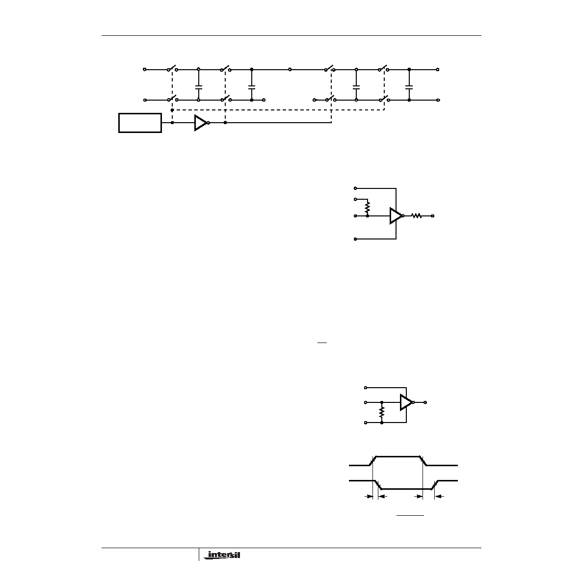
Charge Pump
An equivalent circuit of the charge pump is illustrated in Figure
1. The charge pump contains two sections: the voltage dou-
bler and the voltage inverter. Each section is driven by a two
phase, internally generated clock to generate +10V and -10V.
The nominal clock frequency is 16kHz. During phase one of
the clock, capacitor C1 is charged to VCC. During phase two,
the voltage on C1 is added to VCC, producing a signal across
C3 equal to twice VCC. During phase one, C2 is also charged
to 2VCC, and then during phase two, it is inverted with respect
to ground to produce a signal across C4 equal to -2VCC. The
charge pump accepts input voltages up to 5.5V. The output
impedance of the voltage doubler section (V+) is approxi-
mately 200
, and the output impedance of the voltage
inverter section (V-) is approximately 450
. A typical applica-
tion uses 1
F capacitors for C1-C4, however, the value is not
critical. Increasing the values of C1 and C2 will lower the out-
put impedance of the voltage doubler and inverter, increasing
the values of the reservoir capacitors, C3 and C4, lowers the
ripple on the V+ and V- supplies.
During shutdown mode (HIN230, 236, 240 and 241), SHUT-
DOWN control line set to logic “1”, the charge pump is
turned off, V+ is pulled down to VCC, V- is pulled up to GND,
and the supply current is reduced to less than 10
A. The
transmitter outputs are disabled and the receiver outputs are
placed in the high impedance state.
Transmitters
The transmitters are TTL/CMOS compatible inverters which
translate the inputs to RS-232 outputs. The input logic thresh-
old is about 26% of VCC, or 1.3V for VCC = 5V. A logic 1 at the
input results in a voltage of between -5V and V- at the output,
and a logic 0 results in a voltage between +5V and (V+ -0.6V).
Each transmitter input has an internal 400k
pullup resistor
so any unused input can be left unconnected and its output
remains in its low state. The output voltage swing meets the
RS-232C specifications of
±5V minimum with the worst case
conditions of: all transmitters driving 3k
minimum load
impedance, VCC = 4.5V, and maximum allowable operating
temperature. The transmitters have an internally limited output
slew rate which is less than 30V/
s. The outputs are short cir-
cuit protected and can be shorted to ground indefinitely. The
powered down output impedance is a minimum of 300
with
±2V applied to the outputs and VCC = 0V.
Receivers
The receiver inputs accept up to
±30V while presenting the
required 3k
to 7k input impedance even it the power is off
(VCC = 0V). The receivers have a typical input threshold of
1.3V which is within the
±3V limits, known as the transition
region, of the RS-232 specications. The receiver output is
0V to VCC. The output will be low whenever the input is
greater than 2.4V and high whenever the input is oating or
driven between +0.8V and -30V. The receivers feature 0.5V
hysteresis to improve noise rejection. The receiver Enable
line EN, when set to logic “1”, (HIN236, 239, 240, and 241)
disables the receiver outputs, placing them in the high
impedance mode. The receiver outputs are also placed in
the high impedance state when in shutdown mode.
+
-
C1
+
-
C3
+
-
C2
+
-
C4
S1
S2
S5
S6
S3
S4
S7
S8
VCC
GND
RC
OSCILLATOR
VCC
GND
V+ = 2VCC
GND
V- = -(V+)
C1+
C1
-
C2-
C2+
VOLTAGE INVERTER
VOLTAGE DOUBLER
FIGURE 1. CHARGE PUMP
TOUT
V- < VTOUT < V+
300
400k
TXIN
GND < TXIN < VCC
V-
V+
VCC
FIGURE 2. TRANSMITTER
ROUT
GND < VROUT < VCC
5k
RXIN
-30V < RXIN < +30V
GND
VCC
FIGURE 3. RECEIVER
TIN
VOL
tPLH
tPHL
Average Propagation Delay =
tPHL + tPLH
2
OR
RIN
TOUT
OR
ROUT
FIGURE 4. PROPAGATION DELAY DEFINITION
HIN230 thru HIN241
相关PDF资料 |
PDF描述 |
|---|---|
| HIN238ECB-T | QUAD LINE TRANSCEIVER, PDSO24 |
| HIN238ECA-T | QUAD LINE TRANSCEIVER, PDSO24 |
| HIP0045AB | 1.75 A 8 CHANNEL, LATCH BASED PRPHL DRVR, PDSO20 |
| HIP0050IB | 0.3 A BUF OR INV BASED PRPHL DRVR, PDSO24 |
| HIP1030AS | 1.6 A BUF OR INV BASED PRPHL DRVR, PSFM5 |
相关代理商/技术参数 |
参数描述 |
|---|---|
| HIN239 | 制造商:ISSI 制造商全称:Integrated Silicon Solution, Inc 功能描述:+5V Powered RS-232 Transmitters/Receivers |
| HIN239CB | 功能描述:IC 3DRVR/5RCV RS232 5/12V 24SOIC RoHS:否 类别:集成电路 (IC) >> 接口 - 驱动器,接收器,收发器 系列:- 标准包装:1,000 系列:- 类型:收发器 驱动器/接收器数:2/2 规程:RS232 电源电压:3 V ~ 5.5 V 安装类型:表面贴装 封装/外壳:16-SOIC(0.295",7.50mm 宽) 供应商设备封装:16-SOIC 包装:带卷 (TR) |
| HIN239CB-T | 功能描述:IC 3DRVR/5RCV RS232 5/12V 24SOIC RoHS:否 类别:集成电路 (IC) >> 接口 - 驱动器,接收器,收发器 系列:- 标准包装:1,000 系列:- 类型:收发器 驱动器/接收器数:2/2 规程:RS232 电源电压:3 V ~ 5.5 V 安装类型:表面贴装 封装/外壳:16-SOIC(0.295",7.50mm 宽) 供应商设备封装:16-SOIC 包装:带卷 (TR) |
| HIN239CBZ | 功能描述:RS-232接口集成电路 RS232 5V/12V 3D/5R 1UF CAPS 24 COM RoHS:否 制造商:Exar 数据速率:52 Mbps 工作电源电压:5 V 电源电流:300 mA 工作温度范围:- 40 C to + 85 C 安装风格:SMD/SMT 封装 / 箱体:LQFP-100 封装: |
| HIN239CBZ-T | 功能描述:RS-232接口集成电路 RS232 5V/12V 3D/5R 1UF CAPS 24 COMEL RoHS:否 制造商:Exar 数据速率:52 Mbps 工作电源电压:5 V 电源电流:300 mA 工作温度范围:- 40 C to + 85 C 安装风格:SMD/SMT 封装 / 箱体:LQFP-100 封装: |
发布紧急采购,3分钟左右您将得到回复。