- 您现在的位置:买卖IC网 > Datasheet目录40 > HIP1011BCB-T (Intersil)IC CTRLR HOT PLUG PCI 16-SOIC Datasheet资料下载
参数资料
| 型号: | HIP1011BCB-T |
| 厂商: | Intersil |
| 文件页数: | 7/9页 |
| 文件大小: | 237K |
| 描述: | IC CTRLR HOT PLUG PCI 16-SOIC |
| 标准包装: | 2,500 |
| 类型: | 热交换控制器 |
| 应用: | 通用型 CompactPCI? |
| 内部开关: | 无 |
| 电源电压: | 10.8 V ~ 13.2 V |
| 工作温度: | 0°C ~ 70°C |
| 安装类型: | 表面贴装 |
| 封装/外壳: | 16-SOIC(0.154",3.90mm 宽) |
| 供应商设备封装: | 16-SOIC |
| 包装: | 带卷 (TR) |
7
FN4640.5
November 18, 2004
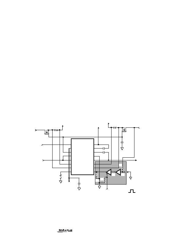
Applications
Implementing the HIP1011B in the CompactPCI
Hot Swap Application
This application offers to the CompactPCI peripheral board
designer programmable Over Current (OC) protection,
programmable delays to latch off, and soft start ramp turn on
for all four supplies with simultaneous latch off upon OC fault
detection.
Figure 6 illustrates the HIP1011EVAL2 evaluation board for
CompactPCI Hot Swap implementation. The shaded
components are the external components necessary to
accomplish both controlled power up and turn-on. For
minimum PCB area single gate logic can be used.
Insertion Sequence
Because of the staggered pin lengths in the CompactPCI
connector, as the board is inserted into the slot, the ground
bus plane is connected first via the longest pins referencing
the HIP1011B by way of the PWRON, OCSET and GND pins
through R4 and R3. Additionally the three-state driver, U1
address line is referenced through R6.
Subsequently the medium length pins engage to connect the
+3.3V, +5V, +12V, -12V lines to the inputs, activating the
HIP1011B, and the 2 logic devices, U1 and U2. At this time the
HIP1011B is in control holding off all the MOSFET switches, as
PWRON is being held low. With the logic devices powered the
inverter U2 input is pulled high putting a low on the three-state
driver U1 input which is passed through to the PWRON pin.
Upon complete insertion the shortest length pin,
board
present
which is tied to ground on the backplane finally
contacts the inverter input. The inverter output pulls high
turning on the HIP1011B through U1 thus, the board is fully
powered on only upon complete insertion.
Fault Reset
If an overcurrent condition is detected on the board by the
HIP1011B the FLTN signal transitions low, once the
V
FLTN,TH
is reached all the switches are simultaneously
switched off protecting the system, the board and its
components. The system controller is notified of the fault
occurrence by the FLTN signal.
Reset of the faulted card is accomplished by a positive pulse
on the three-state oe
input. The pulse puts U1 output into a
high Z state allowing R4 to pull the HIP1011B PWRON pin
low, resetting the HIP1011B. The HIP1011B switches turn
back on when U1 oe
input returns to a low state resulting in
PWRON going high. The reset pulse can be generated by
either the system restart/reset to the master board or from
the master system board to any of the peripheral boards in
the system.
Q1, Q2
C2
Q3, Q4
R3
C3
C4
C1
M12VIN
FLTN
3V5VG
V
CC
12VIN
3VISEN
3VS
OCSET
M12VO
12VG
GND
12VO
5VISEN
5VS
PWRON
M12VG
HIP1011
12V INPUT
5V INPUT
-12V INPUT
R1
3.3V INPUT
R2
FLTN
3.3VOUT
5VOUT
-12V
OUT
+12VOUT
PULSE HIGH TO RESET FAULT
oe
BOARD PRESENT
PIN ON
BACKPLANE
R4
R6
U1
U2
R5
FIGURE 6. HIP1011B CompactPCI APPLICATION CIRCUIT
NOTES:
3. Each test point (TP) on HIP1011EVAL2 refers to device pin number.
4. SIGNAL_GND, SHIELD_GND and SHORTPIN_GND can be jumpered together for ease of evaluation.
5. HIP1011B devices can be placed into HIP1011EVAL2 board for evaluation or contact INTERSIL for a HIP1011B equipped evaluation board.
HIP1011B
相关PDF资料 |
PDF描述 |
|---|---|
| HIP1020CK-T | IC CTRLR HOT PLUG SOT23-5 |
| HIP6018BCBZ-T | IC REG TRPL BCK/LINEAR 24-SOIC |
| HIP6021CB-T | IC REG QD BCK/LINEAR 28-SOIC |
| HIP6521CB-T | IC REG QD BCK/LINEAR SYNC 16SOIC |
| HMC920LP5E | IC CTRLR ACTIVE BIAS 32QFN |
相关代理商/技术参数 |
参数描述 |
|---|---|
| HIP1011BCBZA | 功能描述:热插拔功率分布 W/ANNEAL PCI HOT PLUG PWR CNTRLR RoHS:否 制造商:Texas Instruments 产品:Controllers & Switches 电流限制: 电源电压-最大:7 V 电源电压-最小:- 0.3 V 工作温度范围: 功率耗散: 安装风格:SMD/SMT 封装 / 箱体:MSOP-8 封装:Tube |
| HIP1011BCBZA-T | 功能描述:热插拔功率分布 W/ANNEAL PCI HOT PLUG PWR CNTRLR RoHS:否 制造商:Texas Instruments 产品:Controllers & Switches 电流限制: 电源电压-最大:7 V 电源电压-最小:- 0.3 V 工作温度范围: 功率耗散: 安装风格:SMD/SMT 封装 / 箱体:MSOP-8 封装:Tube |
| HIP1011CB | 功能描述:IC CTRLR HOT PLUG PCI 16-SOIC RoHS:否 类别:集成电路 (IC) >> PMIC - 热交换 系列:- 产品培训模块:Obsolescence Mitigation Program 标准包装:100 系列:- 类型:热插拔开关 应用:通用 内部开关:是 电流限制:可调 电源电压:9 V ~ 13.2 V 工作温度:-40°C ~ 150°C 安装类型:表面贴装 封装/外壳:10-WFDFN 裸露焊盘 供应商设备封装:10-TDFN-EP(3x3) 包装:管件 |
| HIP1011CB-T | 功能描述:IC CTRLR HOT PLUG PCI 16-SOIC RoHS:否 类别:集成电路 (IC) >> PMIC - 热交换 系列:- 产品培训模块:Obsolescence Mitigation Program 标准包装:100 系列:- 类型:热插拔开关 应用:通用 内部开关:是 电流限制:可调 电源电压:9 V ~ 13.2 V 工作温度:-40°C ~ 150°C 安装类型:表面贴装 封装/外壳:10-WFDFN 裸露焊盘 供应商设备封装:10-TDFN-EP(3x3) 包装:管件 |
| HIP1011CB-TS2568 | 制造商:Rochester Electronics LLC 功能描述: 制造商:Intersil Corporation 功能描述: |
发布紧急采购,3分钟左右您将得到回复。