- 您现在的位置:买卖IC网 > PDF目录19713 > HIP1011DCA (Intersil)IC CTRLR HOTPLUG PCI DUAL 28SSOP PDF资料下载
参数资料
| 型号: | HIP1011DCA |
| 厂商: | Intersil |
| 文件页数: | 8/15页 |
| 文件大小: | 0K |
| 描述: | IC CTRLR HOTPLUG PCI DUAL 28SSOP |
| 标准包装: | 48 |
| 类型: | 热交换控制器 |
| 应用: | 通用型 CompactPCI? |
| 内部开关: | 无 |
| 电源电压: | 10.8 V ~ 13.2 V |
| 工作温度: | 0°C ~ 70°C |
| 安装类型: | 表面贴装 |
| 封装/外壳: | 28-SSOP(0.154",3.90mm 宽) |
| 供应商设备封装: | 28-SSOP/QSOP |
| 包装: | 管件 |
�� �
�
�HIP1011D,� HIP1011E�
�TABLE� 1.�
�discharge� the� load� when� disabled.� Upon� turn-off� these�
�SUPPLY�
�+3.3V� I� OC�
�+5.0V� I� OC�
�+12V� I� OC�
�-12V� I� OC�
�HOW� TO� DETERMINE� +25c� NOMINAL� (� ±� 10%)� I� OC�
�FOR� EACH� SUPPLY�
�((100� μ� A� x� R� OCSET� )/11.5)/R� RSENSE�
�((100� μ� A� x� R� OCSET� )/14.5)/R� RSENSE�
�(100� μ� A� x� R� OCSET� )/1�
�(100� μ� A� x� R� OCSET� )/3.4�
�internal� switches� on� each� output� discharge� the� load�
�capacitance� pulling� the� output� to� GND.� These� switches� are�
�also� on� when� PWRON� is� low� thus� an� open� slot� is� held� at� the�
�GND� level.�
�Decoupling� Precautions� and� Recommendations�
�For� the� HIP1011D/E� proper� decoupling� is� a� particular�
�concern� during� the� normal� switching� operation� and�
�Time� Delay� to� Latch-Off�
�Time� delay� to� latch-off� allows� for� a� predetermined� delay� from�
�an� OC� or� UV� in� the� HIP1011D� or� an� OC� in� the� HIP1011E�
�event� to� the� simultaneous� latch-off� of� all� four� supply� switches�
�of� the� affected� slot.� This� delay� period� is� set� by� the�
�capacitance� value� to� ground� from� the� FLTN� pins� for� each�
�slot.� This� capacitance� value� tailors� the� FLTN� signal� going� low�
�ramp� rate.� This� provides� a� delay� to� the� fault� signal� latch-off�
�threshold� voltage,� FLTN,� Vth.� By� increasing� this� time,� the�
�HIP1011D/E� delays� immediate� latch-off� of� the� bus� supply�
�switches,� thus� ignoring� transient� faults.� See� additional�
�information� in� the� “Using� the� HIP1011DEVAL1� Platform”�
�section� of� this� data� sheet.� The� HIP1011E� has� all� features� of�
�the� HIP1011D� but� it� does� not� respond� to� UV� events.�
�Caution:� The� primary� purpose� of� a� protection� device� such�
�as� the� HIP1011D/E� is� to� quickly� isolate� a� faulted� card� from�
�the� voltage� bus.� Delaying� the� time� to� latch-off� works� against�
�this� primary� concern� so� care� must� be� taken� when� using� this�
�feature.� Ensure� adequate� sizing� of� external� FETs� to� carry�
�additional� current� during� time� out� period.� Understand� that�
�especially� during� a� card� crowbar� failure.� If� a� card�
�experiences� a� crow� bar� short� to� ground,� the� supply� to� the�
�other� card� will� experience� transients� until� the� faulted� card� is�
�isolated� from� the� bus.� In� addition� the� common� IC� nodes�
�between� the� two� sides� can� fluctuate� unpredictably� resulting�
�in� a� false� latch-off� of� the� second� slot.� Additionally� to� the�
�mother� board� bulk� capacitance,� it� is� recommended� that� 10� μ� F�
�capacitors� be� placed� on� both� the� +12V� and� -12V� lines� of� the�
�HIP1011D/E� as� close� to� the� chip� as� possible.�
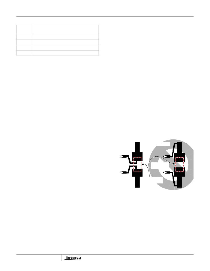
�Recommended� PCB� Layout� Design� Best� Practices�
�To� ensure� accurate� current� sensing,� PCB� traces� that�
�connect� each� of� the� current� sense� resistors� to� the�
�HIP1011D/E� must� not� carry� any� load� current.� This� can� be�
�accomplished� by� two� dedicated� PCB� kelvin� traces� directly�
�from� the� sense� resistors� to� the� HIP1011D/E� (see� examples�
�of� correct� and� incorrect� layouts� below� in� Figure� 3).� To� reduce�
�parasitic� inductance� and� resistance� effects,� maximize� the�
�width� of� the� high-current� PCB� traces.�
�voltage� bus� disruptions� must� be� minimized� for� the� time� delay�
�period� in� the� event� of� a� crow� bar� failure.�
�Devices� using� an� unadjustable� preset� delay� to� latch-off� time�
�present� the� user� with� the� inability� to� eliminate� these�
�concerns� increasing� cost� and� the� chance� of� additional� ripple�
�through� failures.�
�HIP1011D,� HIP1011E� Soft� Start� and� Turn-Off�
�Considerations�
�The� HIP1011D/E� does� allow� the� user� to� select� the� rate� of�
�ramp� up� on� the� voltage� supplies.� This� startup� ramp�
�minimizes� in-rush� current� at� startup� while� the� on� card� bulk�
�CORRECT�
�TO� HIP1011D/E�
�VS� AND� VISEN�
�INCORRECT�
�TO� HIP1011D�
�VS AND VISEN�
�CURRENT�
�SENSE RESISTOR�
�capacitors� charge.� The� ramp� is� created� by� placing�
�capacitors� on� M12VG� to� M12VO,� 12VG� to� 12VO� and� 3V5VG�
�to� ground.� These� capacitors� are� each� charged� up� by� a�
�nominal� 25� μ� A� current� during� turn� on.� The� same� value� for� all�
�gate� timing� capacitors� is� recommended.� A� recommended�
�minimum� value� of� 0.033� μ� F� as� a� smaller� value� may� cause�
�overcurrent� faults� at� power� up.� This� recommendation� results�
�in� a� nominal� gate� voltage� ramp� rate� of� 0.76V/ms.� The� gate�
�capacitors� must� be� discharged� when� a� fault� is� detected� to�
�turn� off� the� power� FETs.� Thus,� larger� caps� slow� the� response�
�time.� If� the� gate� capacitors� are� too� large� the� HIP1011D/E�
�may� not� be� able� to� adequately� protect� the� bus� or� the� power�
�FETs.� The� HIP1011D/E� have� internal� discharge� FETs� to�
�8�
�FIGURE� 3.� SENSE� RESISTOR� PCB� LAYOUT�
�FN4725.5�
�November� 18,� 2004�
�相关PDF资料 |
PDF描述 |
|---|---|
| MIC3975-1.65BMM TR | IC REG LDO 1.65V .75A 8-MSOP |
| V24A36E400B3 | CONVERTER MOD DC/DC 36V 400W |
| MIC3975-1.65BMM | IC REG LDO 1.65V .75A 8-MSOP |
| HIP1011CB-T | IC CTRLR HOT PLUG PCI 16-SOIC |
| 181-015-113R531 | CONN DB15 MALE HI DENSITY R/A |
相关代理商/技术参数 |
参数描述 |
|---|---|
| HIP1011DCA-T | 功能描述:IC CTRLR HOTPLUG PCI DUAL 28SSOP RoHS:否 类别:集成电路 (IC) >> PMIC - 热交换 系列:- 产品培训模块:Obsolescence Mitigation Program 标准包装:100 系列:- 类型:热插拔开关 应用:通用 内部开关:是 电流限制:可调 电源电压:9 V ~ 13.2 V 工作温度:-40°C ~ 150°C 安装类型:表面贴装 封装/外壳:10-WFDFN 裸露焊盘 供应商设备封装:10-TDFN-EP(3x3) 包装:管件 |
| HIP1011DCAZA | 功能描述:热插拔功率分布 W/ANNEAL DL VER OF HIP1011 2 8LD SSOP RoHS:否 制造商:Texas Instruments 产品:Controllers & Switches 电流限制: 电源电压-最大:7 V 电源电压-最小:- 0.3 V 工作温度范围: 功率耗散: 安装风格:SMD/SMT 封装 / 箱体:MSOP-8 封装:Tube |
| HIP1011DCAZA-T | 功能描述:热插拔功率分布 W/ANNEAL DL PCI HOT PLUG PWR CNTRLR RoHS:否 制造商:Texas Instruments 产品:Controllers & Switches 电流限制: 电源电压-最大:7 V 电源电压-最小:- 0.3 V 工作温度范围: 功率耗散: 安装风格:SMD/SMT 封装 / 箱体:MSOP-8 封装:Tube |
| HIP1011DEVAL1 | 功能描述:电源管理IC开发工具 DL SLOT PCI HOT PLUG EVALUATION BRD RoHS:否 制造商:Maxim Integrated 产品:Evaluation Kits 类型:Battery Management 工具用于评估:MAX17710GB 输入电压: 输出电压:1.8 V |
| HIP1011E | 制造商:未知厂家 制造商全称:未知厂家 功能描述:Dual Slot PCI Hot Plug Controller |
发布紧急采购,3分钟左右您将得到回复。