- 您现在的位置:买卖IC网 > PDF目录19712 > HIP1012ACB (Intersil)IC CTRLRL HOT PLUG DUAL 14-SOIC PDF资料下载
参数资料
| 型号: | HIP1012ACB |
| 厂商: | Intersil |
| 文件页数: | 6/15页 |
| 文件大小: | 0K |
| 描述: | IC CTRLRL HOT PLUG DUAL 14-SOIC |
| 标准包装: | 50 |
| 类型: | 热交换控制器 |
| 应用: | 通用 |
| 内部开关: | 无 |
| 电源电压: | 10.5 V ~ 13.2 V |
| 工作温度: | 0°C ~ 70°C |
| 安装类型: | 表面贴装 |
| 封装/外壳: | 14-SOIC(0.154",3.90mm 宽) |
| 供应商设备封装: | 14-SOICN |
| 包装: | 管件 |
�� �
�
�HIP1012A�
�R� ILIM� RESISTOR�
�TABLE� 1.�
�NOMINAL� OC� VTH�
�and� motor� startup� currents,� choosing� the� current� limiting� level�
�is� crucial� to� provide� both� protection� and� still� allow� for� this�
�inrush� current� without� latching� off.� Consider� this� in� addition� to�
�15k� ?�
�10k� ?�
�7.5k� ?�
�4.99k� ?�
�NOTE:� Nominal� OC� Vth� =� Rilim� x� 10� μ� A.�
�TABLE� 2.�
�150mV�
�100mV�
�75mV�
�50mV�
�the� time� out� delay� when� choosing� MOSFETs� for� your� design.�
�To� these� ends� it� is� suggested� that� CR� levels� be� programmed�
�to� 150%� of� nominal� load.�
�When� using� the� HIP1012A� in� the� 12V� and� 5V� mode�
�additional� V� DD� decoupling� may� be� necessary� to� prevent� a�
�power� on� reset� due� to� a� sag� on� V� DD� pin� upon� an� OC� latch� off.�
�The� addition� of� a� capacitor� from� V� DD� to� GND� may� often� be�
�adequate� but� a� small� value� isolation� resistor� may� also� be�
�necessary� (see� the� Simplified� Block� Diagram� on� page� 2).�
�Current� loop� stabilization� is� facilitated� through� a� small� value�
�C� TIM� CAPACITOR�
�0.022� μ� F�
�0.047� μ� F�
�NOMINAL� TIME� OUT� PERIOD�
�4.4ms�
�9.4ms�
�resistor� in� series� with� the� gate� timing� capacitor.� As� the�
�HIP1012A� drives� a� highly� inductive� current� load,� instability�
�characterized� by� the� gate� voltage� repeatedly� ramping� up� and�
�down� may� appear.� A� simple� method� to� enhance� stability� is�
�provided� by� the� substitution� of� a� larger� value� gate� resistor.�
�0.1� μ� F� 20ms�
�NOTE:� Nominal� time-out� period� in� seconds� =� C� TIM� x� 200k� ?.�
�The� HIP1012A� responds� to� a� load� short� (defined� as� a� current�
�level� 3X� the� OC� set� point)� immediately,� driving� the� relevant�
�N-Channel� MOSFET� gate� to� 0V� in� less� than� 10� μ� s.� The� gate�
�voltage� is� then� slowly� ramped� up� turning� on� the� N-Channel�
�MOSFET� to� the� programmed� current� limit� level;� this� is� the�
�start� of� the� time� out� period.� The� programmed� current� level� is�
�held� until� either� the� OC� event� passes� or� the� time� out� period�
�expires.� If� the� former� is� the� case� then� the� N-Channel�
�MOSFET� is� fully� enhanced� and� the� C� TIM� charging� current� is�
�diverted� away� from� the� capacitor.� If� the� time� out� period� expires�
�prior� to� OC� resolution� then� both� gates� are� quickly� pulled� to� 0V�
�turning� off� both� N-Channel� MOSFETs� simultaneously.�
�Upon� any� UV� condition� the� PGOOD� signal� will� pull� low� when�
�tied� high� through� a� resistor� to� the� logic� supply.� This� pin� is� a�
�fault� indicator� but� not� the� OC� latch� off� indicator.� For� an� OC�
�latch� off� indication,� monitor� CTIM,� pin� 10.� This� pin� will� rise�
�rapidly� to� 12V� once� the� time� out� period� expires.� See� Simplified�
�Block� Diagram� on� page� 2� for� OC� latch� off� circuit� suggestion.�
�The� HIP1012A� is� reset� by� a� rising� edge� on� either� PWRON� pin�
�and� is� turned� on� by� either� PWRON� pin� being� driven� low.� The�
�HIP1012A� can� control� either� +12V/5V� or� +3.3V/+5V� supplies.�
�Typically� this� situation� can� be� avoided� by� eliminating� long�
�point� to� point� wiring� to� the� load.�
�Random� resets� occur� if� the� HIP1012A� sense� pins� are� pulled�
�below� ground� when� turning� off� a� highly� inductive� load.� Place� a�
�large� load� capacitor� (10-50� μ� F)� on� the� output� or� ISEN�
�clamping� diodes� to� ground� to� eliminate.�
�During� the� Time� Out� delay� period� with� the� HIP1012A� in�
�current� limit� mode,� the� V� GS� of� the� external� N-Channel�
�MOSFETs� is� reduced� driving� the� N-Channel� MOSFET� switch�
�into� a� high� r� DS(ON)� state.� Thus� avoid� extended� time� out�
�periods� as� the� external� N-Channel� MOSFETs� may� be�
�damaged� or� destroyed� due� to� excessive� internal� power�
�dissipation.� Refer� to� the� MOSFET� manufacturer’s� data� sheet�
�for� SOA� information.�
�External� Pull� Down� resistors� from� the� xISEN� pins� to� ground�
�will� prevent� the� voltage� outputs� from� floating� up� due� to�
�leakage� current� through� the� external� switch� FET� body� diode�
�when� the� FETs� are� disabled� and� the� outputs� are� open.�
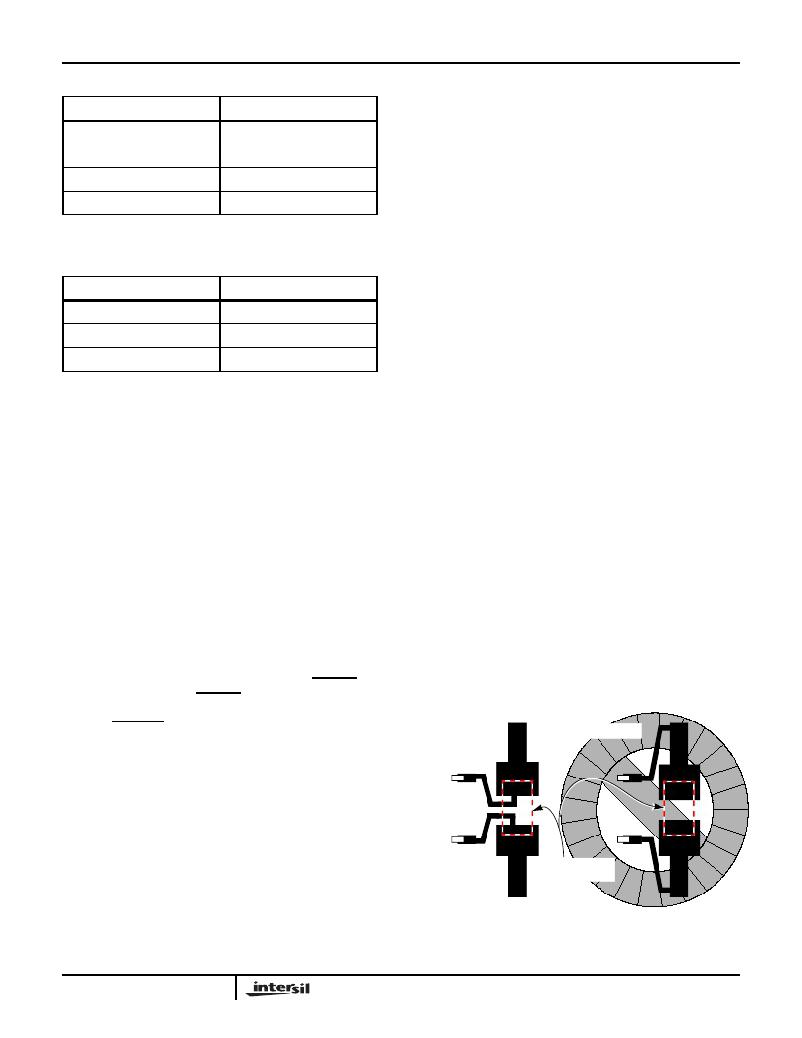
�Physical� layout� of� Rsense� resistors� is� critical� to� avoid� the�
�possibility� of� false� overcurrent� occurrences.� Ideally� trace�
�routing� between� the� Rsense� resistors� and� the� HIP1012A� is�
�direct� and� as� short� as� possible� with� zero� current� in� the� sense�
�lines� as� shown� below� .�
�Tying� the� PWRON1� pin� to� V� DD� ,� invokes� the� +3.3V/+5V�
�voltage� mode.� In� this� mode,� the� external� charge� pump�
�capacitor� is� not� needed� and� Cpump,� pin� 11� is� tied� directly� to�
�V� DD� .�
�HIP1012A� Application� Considerations�
�Current� Regulation� vs� current� trip� often� causes� confusion�
�when� using� this� and� other� ICs� with� a� Current� Regulation� (CR)�
�feature.� The� CR� level� is� the� level� at� which� the� HIP1012� will�
�hold� an� overcurrent� load� for� the� programmed� duration.� This�
�level� is� programmable� by� the� RLIM� and� RSENSE� resistors�
�values.� As� the� current� being� monitored� by� the� HIP1012A�
�approaches� a� level� >85%� of� the� CR� level� the� HIP1012A� may�
�CORRECT�
�TO� ISEN� AND�
�R� ISET�
�INCORRECT�
�CURRENT�
�SENSE RESISTOR�
�trip-off� due� to� variances� in� manufacturing� and� the� design� of�
�the� low� gain� high� speed� input� comparators.� In� addition� with�
�the� high� levels� of� inrush� current� e.g.,� highly� capacitive� loads�
�6�
�FIGURE� 1.� SENSE� RESISTOR� PCB� LAYOUT�
�相关PDF资料 |
PDF描述 |
|---|---|
| 180-015-213R021 | CONN DB15 FEML HD DIP SLD NICKEL |
| HIP1011ECA-T | IC CTRLR HOTPLUG DUAL 28-SSOP |
| HIP1011ECA | IC CTRLR HOTPLUG DUAL 28-SSOP |
| 180-015-213R031 | CONN DB15 FEML HD DIP SLD NICKEL |
| V24A36E400BL3 | CONVERTER MOD DC/DC 36V 400W |
相关代理商/技术参数 |
参数描述 |
|---|---|
| HIP1012ACB-T | 功能描述:IC CTRLRL HOT PLUG DUAL 14-SOIC RoHS:否 类别:集成电路 (IC) >> PMIC - 热交换 系列:- 产品培训模块:Obsolescence Mitigation Program 标准包装:100 系列:- 类型:热插拔开关 应用:通用 内部开关:是 电流限制:可调 电源电压:9 V ~ 13.2 V 工作温度:-40°C ~ 150°C 安装类型:表面贴装 封装/外壳:10-WFDFN 裸露焊盘 供应商设备封装:10-TDFN-EP(3x3) 包装:管件 |
| HIP1012ACBTS2490 | 制造商:INTERSIL 功能描述:New |
| HIP1012ACBZA | 功能描述:热插拔功率分布 W/ANNEAL PWR DIST CONTROLLER RoHS:否 制造商:Texas Instruments 产品:Controllers & Switches 电流限制: 电源电压-最大:7 V 电源电压-最小:- 0.3 V 工作温度范围: 功率耗散: 安装风格:SMD/SMT 封装 / 箱体:MSOP-8 封装:Tube |
| HIP1012ACBZAS2695 | 制造商:Intersil Corporation 功能描述:FOR TRACKING PURPOSES ONLY, USES PL CODE D3P - Rail/Tube |
| HIP1012ACBZA-T | 功能描述:热插拔功率分布 W/ANNEAL PWR DIST CONTROLLER RoHS:否 制造商:Texas Instruments 产品:Controllers & Switches 电流限制: 电源电压-最大:7 V 电源电压-最小:- 0.3 V 工作温度范围: 功率耗散: 安装风格:SMD/SMT 封装 / 箱体:MSOP-8 封装:Tube |
发布紧急采购,3分钟左右您将得到回复。