- 您现在的位置:买卖IC网 > PDF目录20557 > HIP2122FRTAZ (Intersil)IC INTERFACE PDF资料下载
参数资料
| 型号: | HIP2122FRTAZ |
| 厂商: | Intersil |
| 文件页数: | 11/16页 |
| 文件大小: | 0K |
| 描述: | IC INTERFACE |
| 标准包装: | 75 |
| 系列: | * |
�� �
�
�HIP2122,� HIP2123�
�Functional� Description�
�Functional� Overview�
�The� HIP2122/23� have� independent� control� inputs,� LI� and� HI,� for�
�each� output;� LO� and� HO.� When� LI� is� low,� LO� is� low� and� likewise,�
�when� HI� is� low,� HO� is� low.� The� output� negative� transitions� occur�
�with� minimal� (and� fixed)� propagation� delays.�
�The� positive� transitions� of� each� output� are� delayed� by� the�
�programmed� delay� as� set� by� RDT.� With� 80k,� the� delay� is�
�nominally� 25ns.� With� 8k,� the� delay� is� nominally� 220ns.� Resistors�
�values� less� than� 8k� and� greater� than� 80k� are� not� recommended.�
�The� delay� time� as� a� function� of� R� DT� is� approximately�
�t� DT� (ns)� =� 2/R� DT� .�
�Delaying� the� rising� edge� but� not� the� falling� edge� of� each� output� is�
�the� technique� that� prevents� shoot-thru.� Please� note� that� there� is�
�no� logic� that� prevents� both� outputs� from� being� on� if� both� inputs�
�are� on� simultaneously.�
�The� enable� pin,� EN,� when� low,� drives� both� outputs� to� a� low� state.�
�When� the� PWM� input� transitions,� it� is� necessary� to� insure� that�
�both� bridge� FETS� are� not� on� at� the� same� time� to� prevent�
�shoot-through� currents� (break� before� make).� The� programmable�
�of� the� high-side� FET,� the� high-side� UV� lockout� may� engage�
�resulting� with� an� unexpected� operation.�
�Application� Information�
�Selecting� the� Boot� Capacitor� Value�
�The� boot� capacitor� value� is� chosen� not� only� to� supply� the� internal�
�bias� current� of� the� high-side� driver� but� also,� and� more�
�significantly,� to� provide� the� gate� charge� of� the� driven� FET� without�
�causing� the� boot� voltage� to� sag� excessively.� In� practice,� the� boot�
�capacitor� should� have� a� total� charge� that� is� about� 20� times� the�
�gate� charge� of� the� driven� power� FET� for� approximately� a� 5%� drop�
�in� voltage� after� the� charge� has� been� transferred� from� the� boot�
�capacitor� to� the� gate� capacitance.�
�The� following� parameters� are� required� to� calculate� the� value� of�
�the� boot� capacitor� for� a� specific� amount� of� voltage� droop.� In� this�
�example,� the� values� used� are� arbitrary.� They� should� be� changed�
�to� comply� with� the� actual� application.�
�V� DD� =� 10V� V� DD� can� be� any� value� between� 7� and� 14VDC�
�V� HB� =� V� DD� -� 0.6V� =� V� HO� High� side� driver� bias� voltage� (V� DD� -� boot� diode�
�voltage)� referenced� to� V� HS�
�dead� time� forces� both� outputs� to� be� off� before� either� of� the�
�bridge� FETs� is� driven� on.� An� 8k� ?� resistor� connected� between� R� DT�
�and� V� SS� results� in� a� nominal� dead� time� of� 250ns.� An� 80k� ?�
�results� with� a� minimum� nominal� dead� time� of� 50ns.� Resistors�
�values� less� than� 8k� and� greater� than� 80k� are� not� recommended.�
�Dead-time� as� a� function� of� R� DT� is� nominally� t� DT� (ns)� =� 2/R� DT� .�
�The� high-side� driver� bias� is� established� by� the� boot� capacitor�
�connected� between� HB� and� HS.� The� charge� on� the� boot� capacitor�
�is� provided� by� the� internal� boot� diode� that� is� connected� to� V� DD� .�
�The� current� path� to� charge� the� boot� capacitor� occurs� when� the�
�low-side� bridge� FET� is� on.� This� charge� current� is� limited� in�
�amplitude� by� the� inherent� resistance� of� the� boot� diode� and� by� the�
�drain-source� voltage� of� the� low-side� FET.� Assuming� that� the� on�
�time� of� the� low-side� FET� is� sufficiently� long� to� fully� charge� the�
�Period� =� 1ms�
�I� HB� =� 100μA�
�R� GS� =� 100k� ?�
�Ripple� =� 5%�
�I� gate_leak� =� 100nA�
�Qgate80V� =� 64nC�
�This� is� the� longest� expected� switching� period�
�Worst� case� high� side� driver� current� when�
�xHO� =� high�
�(this� value� is� specified� for� V� DD� =� 12V� but� the�
�error� is� not� significant)�
�Gate-source� resistor�
�(usually� not� needed)�
�Desired� ripple� voltage� on� the� boot� capacitor�
�(larger� ripple� is� not� recommended)�
�From� the� FET� vendor’s� datasheet�
�From� Figure� 21�
�boot� capacitor,� the� boot� voltage� will� charge� very� close� to� V� DD�
�(less� the� boot� diode� drop� and� the� low-side� FET� on� voltage).�
�When� the� HI� input� transitions� high,� the� high-side� bridge� FET� is�
�driven� on� after� the� delay� time.� Because� the� HS� node� is� connected�
�to� the� source� of� the� high-side� FET,� the� HS� node� will� rise� almost� to�
�the� level� of� the� bridge� voltage� (less� the� conduction� voltage� across�
�the� bridge� FET).� Because� the� boot� capacitor� voltage� is� referenced�
�to� the� source� voltage� of� the� high-side� FET,� the� HB� node� is� V� DD�
�volts� above� the� HS� node� and� the� boot� diode� is� reversed� biased.�
�Because� the� high-side� driver� circuit� is� referenced� to� the� HS� node,�
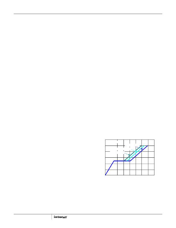
�12�
�10�
�8�
�6�
�4�
�2�
�I� D� =� 33A�
�V� DS� =� 80V�
�V� DS� =� 50V�
�V� DS� =� 20V�
�the� HO� output� is� now� approximately� VHB� +� VBRIDGE� above�
�ground.�
�0�
�0�
�10�
�20�
�30�
�40�
�50�
�60�
�70�
�80�
�During� the� low� to� high� transition� of� the� HS� node,� the� boot�
�capacitor� sources� the� necessary� gate� charge� to� fully� enhance� the�
�high-side� bridge� FET� gate.� After� the� gate� is� fully� charged,� the� boot�
�capacitor� no� longer� sources� the� charge� to� the� gate� but� continues�
�to� provide� bias� current� to� the� high-side� driver.� It� is� clear� that� the�
�charge� of� the� boot� capacitor� must� be� substantially� larger� than�
�the� required� charge� of� the� high-side� FET� and� high-side� driver�
�otherwise� the� boot� voltage� will� sag� excessively.� If� the� boot�
�capacitor� value� is� too� small� for� the� required� maximum� of� on-time�
�11�
�QG� TOTAL� GATE� CHARGE� (nC)�
�FIGURE� 21.� TYPICAL� GATE� CHARGE� OF� A� POWER� FET�
�The� following� equations� calculate� the� total� charge� required� for�
�the� Period.� This� equation� assumes� that� all� of� the� parameters� are�
�constant� during� the� period� duration.� The� error� is� insignificant� if�
�the� ripple� is� small.�
�FN7670.0�
�December� 23,� 2011�
�相关PDF资料 |
PDF描述 |
|---|---|
| LXD75-1400SW | POWER SUPPLY LED DIMMABLE 75W |
| LXC96-1050SW | POWER SUPPLY LED 96W 1050MA |
| AT28C256F-15JA | IC EEPROM 256KBIT 150NS 32PLCC |
| ISL6613BIRZ | IC MOSFET DRVR SYNC BUCK 10-DFN |
| M7PSK-1506J | D-SUB CABLE MMM15K/MC16G/MFM15K |
相关代理商/技术参数 |
参数描述 |
|---|---|
| HIP2122FRTAZ-T | 功能描述:功率驱动器IC 100V 2A PEAK HALF BRDG DRV W/DELAY TMR RoHS:否 制造商:Micrel 产品:MOSFET Gate Drivers 类型:Low Cost High or Low Side MOSFET Driver 上升时间: 下降时间: 电源电压-最大:30 V 电源电压-最小:2.75 V 电源电流: 最大功率耗散: 最大工作温度:+ 85 C 安装风格:SMD/SMT 封装 / 箱体:SOIC-8 封装:Tube |
| HIP2122FRTBZ | 功能描述:功率驱动器IC 100V 2A PEAK HALF BRDG DRV W/DELAY TMR RoHS:否 制造商:Micrel 产品:MOSFET Gate Drivers 类型:Low Cost High or Low Side MOSFET Driver 上升时间: 下降时间: 电源电压-最大:30 V 电源电压-最小:2.75 V 电源电流: 最大功率耗散: 最大工作温度:+ 85 C 安装风格:SMD/SMT 封装 / 箱体:SOIC-8 封装:Tube |
| HIP2122FRTBZ-T | 功能描述:功率驱动器IC 100V 2A PEAK HALF BRDG DRV W/DELAY TMR RoHS:否 制造商:Micrel 产品:MOSFET Gate Drivers 类型:Low Cost High or Low Side MOSFET Driver 上升时间: 下降时间: 电源电压-最大:30 V 电源电压-最小:2.75 V 电源电流: 最大功率耗散: 最大工作温度:+ 85 C 安装风格:SMD/SMT 封装 / 箱体:SOIC-8 封装:Tube |
| HIP2123 | 制造商:INTERSIL 制造商全称:Intersil Corporation 功能描述:100V, 2A Peak, High Frequency Half-Bridge Drivers with Rising Edge Delay Timer |
| HIP2123FRTAZ | 功能描述:功率驱动器IC 100V 2A PEAK HALF BRDG DRV W/DELAY TMR RoHS:否 制造商:Micrel 产品:MOSFET Gate Drivers 类型:Low Cost High or Low Side MOSFET Driver 上升时间: 下降时间: 电源电压-最大:30 V 电源电压-最小:2.75 V 电源电流: 最大功率耗散: 最大工作温度:+ 85 C 安装风格:SMD/SMT 封装 / 箱体:SOIC-8 封装:Tube |
发布紧急采购,3分钟左右您将得到回复。