- 您现在的位置:买卖IC网 > PDF目录371821 > HIP4081IP (HARRIS SEMICONDUCTOR) 80V/2.5A Peak, High Frequency Full Bridge FET Driver PDF资料下载
参数资料
| 型号: | HIP4081IP |
| 厂商: | HARRIS SEMICONDUCTOR |
| 元件分类: | 功率晶体管 |
| 英文描述: | 80V/2.5A Peak, High Frequency Full Bridge FET Driver |
| 中文描述: | 2.6 A FULL BRDG BASED MOSFET DRIVER, PDIP20 |
| 文件页数: | 12/18页 |
| 文件大小: | 216K |
| 代理商: | HIP4081IP |
12
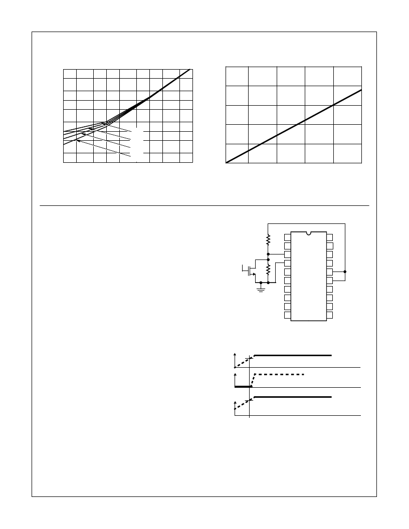
HI4081 Power-up Application Information
The HIP4081 H-Bridge Driver IC requires external circuitry
to assure reliable start-up conditions of the upper drivers. If
not addressed in the application, the H-bridge power MOS-
FETs may be exposed to shoot-through current, possibly
leading to MOSFET failure. Following the instructions below
will result in reliable start-up.
The HIP4081 has four inputs, one for each output. Outputs
ALO and BLO are directly controlled by input ALI and BLI.
By holding ALI and BLI low during start-up no shoot-through
conditions can occur. To set the latches to the upper drivers
such that the driver outputs, AHO and BHO, are off, the DIS
pin must be toggled from low to high after power is applied.
This is accomplished with a simple resistor divider, as shown
below in Figure 30. As the V
DD
/V
CC
supply ramps from zero
up, the DIS voltage is below its input threshold of 1.7V due
to the R1/R2 resistor divider. When V
DD
/V
CC
exceeds
approximately 9V to 10V, DIS becomes greater than the
input threshold and the chip disables all outputs. It is critical
that ALI and BLI be held low prior to DIS reaching its thresh-
old level of 1.7V while V
DD
/V
CC
is ramping up, so that shoot
through is avoided. After power is up the chip can be
enabled by the ENABLE signal which pulls the DIS pin low.
FIGURE 28. HIGH VOLTAGE LEVEL-SHIFT CURRENT vs
FREQUENCY AND BUS VOLTAGE
FIGURE 29. MINIMUM DEAD-TIME vs DEL RESISTANCE
Typical Performance Curves
V
DD
= V
CC
= V
AHB
= V
BHB
= 12V, V
SS
= V
ALS
= V
BLS
= V
AHS
= V
BHS
= 0V,
R
HDEL
= R
LDEL
= 100K and T
A
= 25
o
C, Unless Otherwise Specified
(Continued)
1
10
100
1000
2
5
SWITCHING FREQUENCY (kHz)
20
50
200
500
1
10
100
1000
2
5
20
50
200
500
L
μ
A
60V
40V
80V
20V
10
50
100
150
200
250
0
30
60
90
120
150
HDEL/LDEL RESISTANCE (k
)
D
11
12
13
14
15
16
17
18
20
19
10
9
8
7
6
5
4
3
2
1 BHB
BHI
DIS
V
SS
BLI
ALI
HDEL
AHI
LDEL
AHB
BHO
BLO
BLS
V
DD
V
CC
ALS
BHS
ALO
AHS
AHO
3.3K
R2
ENABLE
R1
15K
FIGURE 30A.
V
DD
DIS
ALI, BLI
t1
8.5V TO 10.5V (ASSUMES 5% RESISTORS)
1.7V
12V, FINAL VALUE
NOTES:
2. ALI and/or BLI may be high after t1, whereupon the ENABLE pin
may also be brought high.
3. Another product, HIP4081A, incorporates undervoltage circuitry
which eliminates the need for the above power up circuitry.
FIGURE 30B. TIMING DIAGRAM FOR FIGURE 30A
HIP4081
相关PDF资料 |
PDF描述 |
|---|---|
| HIP4082IB | 80V, 1.25A Peak Current H-Bridge FET Driver |
| HIP4082 | 80V, 1.25A Peak Current H-Bridge FET Driver |
| HIP4082IP | 30000 SYSTEM GATE 3.3 VOLT LOGIC CELL AR - NOT RECOMMENDED for NEW DESIGN |
| HIP5010IS-T | Output Stage |
| HIP5011IS-T | Output Stage |
相关代理商/技术参数 |
参数描述 |
|---|---|
| HIP4081IPR3162 | 制造商:Rochester Electronics LLC 功能描述:- Bulk |
| HIP4082 | 制造商:INTERSIL 制造商全称:Intersil Corporation 功能描述:80V, 1.25A Peak Current H-Bridge FET Driver |
| HIP4082_06 | 制造商:INTERSIL 制造商全称:Intersil Corporation 功能描述:80V, 1.25A Peak Current H-Bridge FET Driver |
| HIP4082AEVA2 | 制造商:Rochester Electronics LLC 功能描述:- Bulk |
| HIP4082AEVAL2 | 制造商:Rochester Electronics LLC 功能描述:- Bulk |
发布紧急采购,3分钟左右您将得到回复。