- 您现在的位置:买卖IC网 > PDF目录385382 > HIP6004BCV (INTERSIL CORP) Buck and Synchronous-Rectifier (PWM) Controller and Output Voltage Monitor PDF资料下载
参数资料
| 型号: | HIP6004BCV |
| 厂商: | INTERSIL CORP |
| 元件分类: | 稳压器 |
| 英文描述: | Buck and Synchronous-Rectifier (PWM) Controller and Output Voltage Monitor |
| 中文描述: | SWITCHING CONTROLLER, 215 kHz SWITCHING FREQ-MAX, PDSO20 |
| 封装: | PLASTIC, TSSOP-20 |
| 文件页数: | 5/12页 |
| 文件大小: | 339K |
| 代理商: | HIP6004BCV |
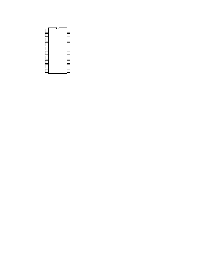
Functional Pin Descriptions
VSEN (Pin 1)
This pin is connected to the converters output voltage. The
PGOOD and OVP comparator circuits use this signal to
report output voltage status and for overvoltage protection.
OCSET (Pin 2)
Connect a resistor (R
OCSET
) from this pin to the drain of
the upper MOSFET. R
OCSET
, an internal 200
μ
A current
source (I
OCS
), and the upper MOSFET on-resistance
(r
DS(ON)
) set the converter over-current (OC) trip point
according to the following equation:
An over-current trip cycles the soft-start function.
SS (Pin 3)
Connect a capacitor from this pin to ground. This capacitor,
along with an internal 10
μ
A current source, sets the soft-
start interval of the converter.
VID0-4 (Pins 4-8)
VID0-4 are the input pins to the 5-bit DAC. The states of
these five pins program the internal voltage reference
(DACOUT). The level of DACOUT sets the converter
output voltage. It also sets the PGOOD and OVP
thresholds. Table 1 specifies DACOUT for the all
combinations of DAC inputs.
COMP (Pin 9) and FB (Pin 10)
COMP and FB are the available external pins of the error
amplifier. The FB pin is the inverting input of the error
amplifier and the COMP pin is the error amplifier output.
These pins are used to compensate the voltage-control
feedback loop of the converter.
GND (Pin 11)
Signal ground for the IC. All voltage levels are measured
with respect to this pin.
PGOOD (Pin 12)
PGOOD is an open collector output used to indicate the
status of the converter output voltage. This pin is pulled low
when the converter output is not within
±
10%
of the
DACOUT reference voltage. Exception to this behavior is
the ‘11111’ VID pin combination which disables the
converter; in this case PGOOD asserts a high level.
PHASE (Pin 13)
Connect the PHASE pin to the upper MOSFET source.
This pin is used to monitor the voltage drop across the
MOSFET for over-current protection. This pin also provides
the return path for the upper gate drive.
UGATE (Pin 14)
Connect UGATE to the upper MOSFET gate. This pin
provides the gate drive for the upper MOSFET.
BOOT (Pin 15)
This pin provides bias voltage to the upper MOSFET driver.
A bootstrap circuit may be used to create a BOOT voltage
suitable to drive a standard N-Channel MOSFET.
PGND (Pin 16)
This is the power ground connection. Tie the lower
MOSFET source to this pin.
LGATE (Pin 17)
Connect LGATE to the lower MOSFET gate. This pin
provides the gate drive for the lower MOSFET.
VCC (Pin 18)
Provide a 12V bias supply for the chip to this pin.
OVP (Pin 19)
The OVP pin can be used to drive an external SCR in the
event of an overvoltage condition. Output rising 15% more
than the DAC-set voltage triggers a high output on this pin
and disables PWM gate drive circuitry.
RT (Pin 20)
This pin provides oscillator switching frequency
adjustment. By placing a resistor (R
T
) from this pin to GND,
the nominal 200kHz switching frequency is increased
according to the following equation:
Conversely, connecting a pull-up resistor (R
T
) from this pin
to V
CC
reduces the switching frequency according to the
following equation:
11
12
13
14
15
16
17
18
20
19
10
9
8
7
6
5
4
3
2
1
VSEN
OCSET
SS
VID0
VID1
VID2
VID4
VID3
COMP
FB
RT
VCC
LGATE
PGND
OVP
BOOT
UGATE
PHASE
PGOOD
GND
I
PEAK
I
x R
DS ON
)
----------------------------------------------------
=
Fs
200kHz
6
T
)
--------------------
+
≈
(R
T
to GND)
Fs
200kHz
7
T
)
--------------------
–
≈
(R
T
to 12V)
HIP6004B
相关PDF资料 |
PDF描述 |
|---|---|
| HIP6004ECBZ | Buck and Synchronous-Rectifier (PWM) Controller and Output Voltage Monitor |
| HIP6004ECVZ | Buck and Synchronous-Rectifier (PWM) Controller and Output Voltage Monitor |
| HIP6004E | Buck and Synchronous-Rectifier (PWM) Controller and Output Voltage Monitor |
| HIP6004ECB | Buck and Synchronous-Rectifier (PWM) Controller and Output Voltage Monitor |
| HIP6004ECV | Buck and Synchronous-Rectifier (PWM) Controller and Output Voltage Monitor |
相关代理商/技术参数 |
参数描述 |
|---|---|
| HIP6004BCV-T | 功能描述:IC CTRLR PWM VOLTAGE MON 20TSSOP RoHS:否 类别:集成电路 (IC) >> PMIC - 稳压器 - 专用型 系列:- 产品培训模块:Lead (SnPb) Finish for COTS Obsolescence Mitigation Program 标准包装:2,000 系列:- 应用:电源,ICERA E400,E450 输入电压:4.1 V ~ 5.5 V 输出数:10 输出电压:可编程 工作温度:-40°C ~ 85°C 安装类型:表面贴装 封装/外壳:42-WFBGA,WLCSP 供应商设备封装:42-WLP 包装:带卷 (TR) |
| HIP6004BCVZ | 功能描述:电压模式 PWM 控制器 BUCK PWM W/ EXTENDED DACRNG RoHS:否 制造商:Texas Instruments 输出端数量:1 拓扑结构:Buck 输出电压:34 V 输出电流: 开关频率: 工作电源电压:4.5 V to 5.5 V 电源电流:600 uA 最大工作温度:+ 125 C 最小工作温度:- 40 C 封装 / 箱体:WSON-8 封装:Reel |
| HIP6004BCVZA | 功能描述:电压模式 PWM 控制器 W/ANNEAL BUCK PWM W/ EXTENED DAC RNG RoHS:否 制造商:Texas Instruments 输出端数量:1 拓扑结构:Buck 输出电压:34 V 输出电流: 开关频率: 工作电源电压:4.5 V to 5.5 V 电源电流:600 uA 最大工作温度:+ 125 C 最小工作温度:- 40 C 封装 / 箱体:WSON-8 封装:Reel |
| HIP6004BCVZA-T | 功能描述:电压模式 PWM 控制器 W/ANNEAL BUCK PWM W/ EXTENED DAC RNG RoHS:否 制造商:Texas Instruments 输出端数量:1 拓扑结构:Buck 输出电压:34 V 输出电流: 开关频率: 工作电源电压:4.5 V to 5.5 V 电源电流:600 uA 最大工作温度:+ 125 C 最小工作温度:- 40 C 封装 / 箱体:WSON-8 封装:Reel |
| HIP6004BCVZ-T | 功能描述:电压模式 PWM 控制器 BUCK PWM W/ EXTENDED DACRNG RoHS:否 制造商:Texas Instruments 输出端数量:1 拓扑结构:Buck 输出电压:34 V 输出电流: 开关频率: 工作电源电压:4.5 V to 5.5 V 电源电流:600 uA 最大工作温度:+ 125 C 最小工作温度:- 40 C 封装 / 箱体:WSON-8 封装:Reel |
发布紧急采购,3分钟左右您将得到回复。