参数资料
| 型号: | HIP6004BCVZ |
| 厂商: | Intersil |
| 文件页数: | 8/15页 |
| 文件大小: | 0K |
| 描述: | IC CTRLR PWM VOLTAGE MON 20TSSOP |
| 标准包装: | 740 |
| 应用: | 控制器,Intel Pentium?,II,Pro |
| 输入电压: | 5V,12V |
| 输出数: | 1 |
| 输出电压: | 1.3 V ~ 3.5 V |
| 工作温度: | 0°C ~ 70°C |
| 安装类型: | 表面贴装 |
| 封装/外壳: | 20-TSSOP(0.173",4.40mm 宽) |
| 供应商设备封装: | 20-TSSOP |
| 包装: | 管件 |
�� �
�
�HIP6004B�
�TABLE� 1.� OUTPUT� VOLTAGE� PROGRAM�
�PIN� NAME�
�NOMINAL� OUTPUT�
�PIN� NAME�
�NOMINAL� OUTPUT�
�VID4�
�0�
�0�
�0�
�0�
�0�
�0�
�0�
�0�
�0�
�0�
�0�
�0�
�0�
�0�
�0�
�0�
�VID3�
�1�
�1�
�1�
�1�
�1�
�1�
�1�
�1�
�0�
�0�
�0�
�0�
�0�
�0�
�0�
�0�
�VID2�
�1�
�1�
�1�
�1�
�0�
�0�
�0�
�0�
�1�
�1�
�1�
�1�
�0�
�0�
�0�
�0�
�VID1�
�1�
�1�
�0�
�0�
�1�
�1�
�0�
�0�
�1�
�1�
�0�
�0�
�1�
�1�
�0�
�0�
�VID0�
�1�
�0�
�1�
�0�
�1�
�0�
�1�
�0�
�1�
�0�
�1�
�0�
�1�
�0�
�1�
�0�
�VOLTAGE� DACOUT�
�1.30�
�1.35�
�1.40�
�1.45�
�1.50�
�1.55�
�1.60�
�1.65�
�1.70�
�1.75�
�1.80�
�1.85�
�1.90�
�1.95�
�2.00�
�2.05�
�VID4�
�1�
�1�
�1�
�1�
�1�
�1�
�1�
�1�
�1�
�1�
�1�
�1�
�1�
�1�
�1�
�1�
�VID3�
�1�
�1�
�1�
�1�
�1�
�1�
�1�
�1�
�0�
�0�
�0�
�0�
�0�
�0�
�0�
�0�
�VID2�
�1�
�1�
�1�
�1�
�0�
�0�
�0�
�0�
�1�
�1�
�1�
�1�
�0�
�0�
�0�
�0�
�VID1�
�1�
�1�
�0�
�0�
�1�
�1�
�0�
�0�
�1�
�1�
�0�
�0�
�1�
�1�
�0�
�0�
�VID0�
�1�
�0�
�1�
�0�
�1�
�0�
�1�
�0�
�1�
�0�
�1�
�0�
�1�
�0�
�1�
�0�
�VOLTAGE� DACOUT�
�0�
�2.1�
�2.2�
�2.3�
�2.4�
�2.5�
�2.6�
�2.7�
�2.8�
�2.9�
�3.0�
�3.1�
�3.2�
�3.3�
�3.4�
�3.5�
�NOTE:� 0� =� connected� to� GND� or� V� SS� ,� 1� =� connected� to� V� DD� through� pull-up� resistors.�
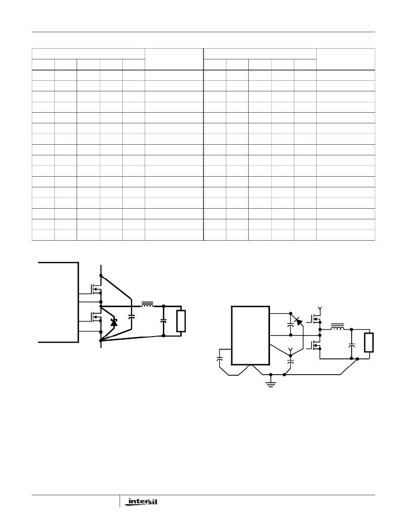
�HIP6004B�
�V� IN�
�current� paths� on� the� SS� PIN� and� locate� the� capacitor,� C� SS�
�close� to� the� SS� pin� because� the� internal� current� source� is�
�only� 10μA.� Provide� local� V� CC� decoupling� between� V� CC� and�
�GND� pins.� Locate� the� capacitor,� C� BOOT� as� close� as�
�UGATE�
�PHASE�
�Q� 1�
�L� O�
�V� OUT�
�practical� to� the� BOOT� and� PHASE� pins.�
�LGATE�
�Q� 2�
�D� 2�
�C� IN�
�C� O�
�BOOT�
�C� BOOT�
�D� 1�
�+V� IN�
�Q� 1�
�L� O�
�V� OUT�
�PGND�
�HIP6004B�
�PHASE�
�RETURN�
�SS�
�V� CC�
�+12V�
�Q� 2�
�C� O�
�FIGURE� 5.� PRINTED� CIRCUIT� BOARD� POWER� AND�
�GROUND� PLANES� OR� ISLANDS�
�Figure� 5� shows� the� critical� power� components� of� the� converter.�
�To� minimize� the� voltage� overshoot� the� interconnecting� wires�
�C� SS�
�GND�
�C� VCC�
�indicated� by� heavy� lines� should� be� part� of� ground� or� power�
�plane� in� a� printed� circuit� board.� The� components� shown� in�
�Figure� 5� should� be� located� as� close� together� as� possible.�
�Please� note� that� the� capacitors� C� IN� and� C� O� each� represent�
�numerous� physical� capacitors.� Locate� the� HIP6004B� within� 3�
�inches� of� the� MOSFETs,� Q� 1� and� Q� 2� .� The� circuit� traces� for� the�
�MOSFETs’� gate� and� source� connections� from� the� HIP6004B�
�must� be� sized� to� handle� up� to� 1A� peak� current.�
�Figure� 6� shows� the� circuit� traces� that� require� additional�
�layout� consideration.� Use� single� point� and� ground� plane�
�construction� for� the� circuits� shown.� Minimize� any� leakage�
�8�
�FIGURE� 6.� PRINTED� CIRCUIT� BOARD� SMALL� SIGNAL�
�LAYOUT� GUIDELINES�
�Feedback� Compensation�
�Figure� 7� highlights� the� voltage-mode� control� loop� for� a�
�synchronous-rectified� buck� converter.� The� output� voltage�
�(V� OUT� )� is� regulated� to� the� Reference� voltage� level.� The�
�error� amplifier� (Error� Amp)� output� (V� E/A� )� is� compared� with�
�the� oscillator� (OSC)� triangular� wave� to� provide� a� pulse-�
�width� modulated� (PWM)� wave� with� an� amplitude� of� V� IN� at�
�the� PHASE� node.�
�相关PDF资料 |
PDF描述 |
|---|---|
| RCC50DRAN-S734 | CONN EDGECARD 100PS .100 R/A PCB |
| ISL6227CAZ-TS2698 | IC CONTROLLER DDR, DDR2 28QSOP |
| RCC50DRAH-S734 | CONN EDGECARD 100PS .100 R/A PCB |
| EL7520ILZ-T7 | IC CTRLR DC/DC 4-CHAN 20-QFN |
| EL7520ILZ-T13 | IC CTRLR DC/DC 4-CHAN 20-QFN |
相关代理商/技术参数 |
参数描述 |
|---|---|
| HIP6004BCVZA | 功能描述:电压模式 PWM 控制器 W/ANNEAL BUCK PWM W/ EXTENED DAC RNG RoHS:否 制造商:Texas Instruments 输出端数量:1 拓扑结构:Buck 输出电压:34 V 输出电流: 开关频率: 工作电源电压:4.5 V to 5.5 V 电源电流:600 uA 最大工作温度:+ 125 C 最小工作温度:- 40 C 封装 / 箱体:WSON-8 封装:Reel |
| HIP6004BCVZA-T | 功能描述:电压模式 PWM 控制器 W/ANNEAL BUCK PWM W/ EXTENED DAC RNG RoHS:否 制造商:Texas Instruments 输出端数量:1 拓扑结构:Buck 输出电压:34 V 输出电流: 开关频率: 工作电源电压:4.5 V to 5.5 V 电源电流:600 uA 最大工作温度:+ 125 C 最小工作温度:- 40 C 封装 / 箱体:WSON-8 封装:Reel |
| HIP6004BCVZ-T | 功能描述:电压模式 PWM 控制器 BUCK PWM W/ EXTENDED DACRNG RoHS:否 制造商:Texas Instruments 输出端数量:1 拓扑结构:Buck 输出电压:34 V 输出电流: 开关频率: 工作电源电压:4.5 V to 5.5 V 电源电流:600 uA 最大工作温度:+ 125 C 最小工作温度:- 40 C 封装 / 箱体:WSON-8 封装:Reel |
| HIP6004CB | 制造商:Rochester Electronics LLC 功能描述:SYNC BUCK PWM W/5 BIT DAC 20 SOIC - Bulk |
| HIP6004CB WAF | 制造商:Harris Corporation 功能描述: |
发布紧急采购,3分钟左右您将得到回复。