- 您现在的位置:买卖IC网 > PDF目录385382 > HIP6004ECV (INTERSIL CORP) Buck and Synchronous-Rectifier (PWM) Controller and Output Voltage Monitor PDF资料下载
参数资料
| 型号: | HIP6004ECV |
| 厂商: | INTERSIL CORP |
| 元件分类: | 稳压器 |
| 英文描述: | Buck and Synchronous-Rectifier (PWM) Controller and Output Voltage Monitor |
| 中文描述: | SWITCHING CONTROLLER, 1000 kHz SWITCHING FREQ-MAX, PDSO20 |
| 封装: | PLASTIC, TSSOP-20 |
| 文件页数: | 7/12页 |
| 文件大小: | 317K |
| 代理商: | HIP6004ECV |
7
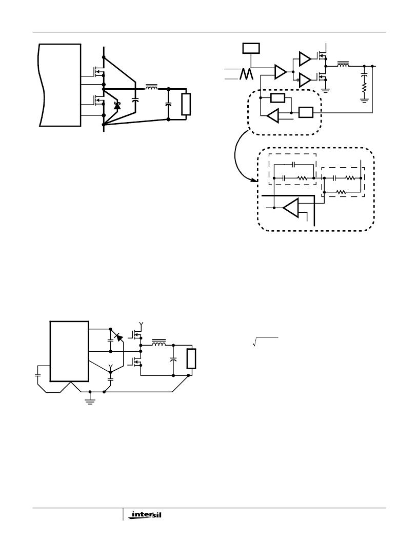
Figure 5 shows the critical power components of the converter.
To minimize the voltage overshoot the interconnecting wires
indicated by heavy lines should be part of ground or power
plane in a printed circuit board. The components shown in
Figure 5 should be located as close together as possible.
Please note that the capacitors C
IN
and C
O
each represent
numerous physical capacitors. Locate the HIP6004E within 3
inches of the MOSFETs, Q
1
and Q
2
. The circuit traces for the
MOSFETs’ gate and source connections from the HIP6004E
must be sized to handle up to 1A peak current.
Figure 6 shows the circuit traces that require additional
layout consideration. Use single point and ground plane
construction for the circuits shown. Minimize any leakage
current paths on the SS pin and locate the capacitor, C
SS
close to the SS pin because the internal current source is
only 10
μ
A. Provide local V
CC
decoupling between VCC and
GND pins. Locate the capacitor, C
BOOT
as close as
practical to the BOOT and PHASE pins.
Feedback Compensation
Figure 7 highlights the voltage-mode control loop for a
synchronous-rectified buck converter. The output voltage
(V
OUT
) is regulated to the Reference voltage level. The
error amplifier (Error Amp) output (V
E/A
) is compared with
the oscillator (OSC) triangular wave to provide a pulse-
width modulated (PWM) wave with an amplitude of V
IN
at
the PHASE node.
The PWM wave is smoothed by the output filter (L
O
and C
O
).
The modulator transfer function is the small-signal transfer
function of V
OUT
/V
E/A
. This function is dominated by a DC
Gain and the output filter (L
O
and C
O
), with a double pole
break frequency at F
LC
and a zero at F
ESR
. The DC Gain of
the modulator is simply the input voltage (V
IN
) divided by the
peak-to-peak oscillator voltage
V
OSC
.
Modulator Break Frequency Equations
The compensation network consists of the error amplifier
(internal to the HIP6004E) and the impedance networks Z
IN
and Z
FB
. The goal of the compensation network is to provide
a closed loop transfer function with the highest 0dB crossing
frequency (f
0dB
) and adequate phase margin. Phase margin
is the difference between the closed loop phase at f
0dB
and
180
degrees
.
The equations below relate the compensation
network’s poles, zeros and gain to the components (R
1
, R
2
,
R
3
, C
1
, C
2
, and C
3
) in Figure 7. Use these guidelines for
locating the poles and zeros of the compensation network:
1. Pick Gain (R
2
/R
1
) for desired converter bandwidth.
2. Place 1
ST
Zero Below Filter’s Double Pole (~75% F
LC
).
3. Place 2
ND
Zero at Filter’s Double Pole.
4. Place 1
ST
Pole at the ESR Zero.
5. Place 2
ND
Pole at Half the Switching Frequency.
6. Check Gain against Error Amplifier’s Open-Loop Gain.
7. Estimate Phase Margin - Repeat if Necessary.
PGND
L
O
C
O
LGATE
UGATE
PHASE
Q
1
Q
2
D
2
V
IN
V
OUT
RETURN
HIP6004E
C
IN
L
FIGURE 5. PRINTED CIRCUIT BOARD POWER AND
GROUND PLANES OR ISLANDS
FIGURE 6. PRINTED CIRCUIT BOARD SMALL SIGNAL
LAYOUT GUIDELINES
+12V
HIP6004E
SS
GND
VCC
BOOT
D
1
L
O
C
O
V
OUT
L
Q
1
Q
2
PHASE
+V
IN
C
BOOT
C
VCC
C
SS
FIGURE 7. VOLTAGE-MODE BUCK CONVERTER
COMPENSATION DESIGN
V
OUT
REFERENCE
L
O
C
O
ESR
V
IN
V
OSC
ERROR
AMP
PWM
DRIVER
(PARASITIC)
Z
FB
+
-
DACOUT
R
1
R
3
R
2
C
3
C
2
C
1
COMP
V
OUT
FB
Z
FB
HIP6004E
Z
IN
COMPARATOR
DRIVER
DETAILED COMPENSATION COMPONENTS
PHASE
V
E/A
+
-
+
-
Z
IN
OSC
FLC
2
π
x LO x CO
------------------------------------------
=
FESR
-------------------------------------------
=
HIP6004E
相关PDF资料 |
PDF描述 |
|---|---|
| HIP6013 | FPGA - 100000 SYSTEM GATE 2.5 VOLT - NOT RECOMMENDED for NEW DESIGN |
| HIP6013CB | FPGA - 100000 SYSTEM GATE 2.5 VOLT - NOT RECOMMENDED for NEW DESIGN |
| HIP6014 | Buck and Synchronous-Rectifier (PWM) Controller and Output Voltage Monitor |
| HIP6014CB | Buck and Synchronous-Rectifier (PWM) Controller and Output Voltage Monitor |
| HIP6016 | FPGA - 100000 SYSTEM GATE 2.5 VOLT - NOT RECOMMENDED for NEW DESIGN |
相关代理商/技术参数 |
参数描述 |
|---|---|
| HIP6004ECV-T | 功能描述:IC CTRLR PWM VOLTAGE MON 20TSSOP RoHS:否 类别:集成电路 (IC) >> PMIC - 稳压器 - 专用型 系列:- 产品培训模块:Lead (SnPb) Finish for COTS Obsolescence Mitigation Program 标准包装:2,000 系列:- 应用:电源,ICERA E400,E450 输入电压:4.1 V ~ 5.5 V 输出数:10 输出电压:可编程 工作温度:-40°C ~ 85°C 安装类型:表面贴装 封装/外壳:42-WFBGA,WLCSP 供应商设备封装:42-WLP 包装:带卷 (TR) |
| HIP6004ECVZ | 功能描述:电压模式 PWM 控制器 20LD BUCK & SYNCHCT PWMCONT & OUTPUT RoHS:否 制造商:Texas Instruments 输出端数量:1 拓扑结构:Buck 输出电压:34 V 输出电流: 开关频率: 工作电源电压:4.5 V to 5.5 V 电源电流:600 uA 最大工作温度:+ 125 C 最小工作温度:- 40 C 封装 / 箱体:WSON-8 封装:Reel |
| HIP6004ECVZ-T | 功能描述:电压模式 PWM 控制器 20LD BUCK&SYNCHCT PWMCONOUTPUT RoHS:否 制造商:Texas Instruments 输出端数量:1 拓扑结构:Buck 输出电压:34 V 输出电流: 开关频率: 工作电源电压:4.5 V to 5.5 V 电源电流:600 uA 最大工作温度:+ 125 C 最小工作温度:- 40 C 封装 / 箱体:WSON-8 封装:Reel |
| HIP6004EVAL1 | 功能描述:EVALUATION BOARD HIP6004 RoHS:否 类别:编程器,开发系统 >> 过时/停产零件编号 系列:- 标准包装:1 系列:- 传感器类型:CMOS 成像,彩色(RGB) 传感范围:WVGA 接口:I²C 灵敏度:60 fps 电源电压:5.7 V ~ 6.3 V 嵌入式:否 已供物品:成像器板 已用 IC / 零件:KAC-00401 相关产品:4H2099-ND - SENSOR IMAGE WVGA COLOR 48-PQFP4H2094-ND - SENSOR IMAGE WVGA MONO 48-PQFP |
| HIP6004EVAL3 | 功能描述:电源管理IC开发工具 EMBEDDED EVAL BRD SYNC BUCK/KLAM RoHS:否 制造商:Maxim Integrated 产品:Evaluation Kits 类型:Battery Management 工具用于评估:MAX17710GB 输入电压: 输出电压:1.8 V |
发布紧急采购,3分钟左右您将得到回复。