- 您现在的位置:买卖IC网 > PDF目录385382 > HIP6004ECVZ (INTERSIL CORP) Buck and Synchronous-Rectifier (PWM) Controller and Output Voltage Monitor PDF资料下载
参数资料
| 型号: | HIP6004ECVZ |
| 厂商: | INTERSIL CORP |
| 元件分类: | 稳压器 |
| 英文描述: | Buck and Synchronous-Rectifier (PWM) Controller and Output Voltage Monitor |
| 中文描述: | SWITCHING CONTROLLER, 1000 kHz SWITCHING FREQ-MAX, PDSO20 |
| 封装: | PLASTIC, TSSOP-20 |
| 文件页数: | 8/13页 |
| 文件大小: | 504K |
| 代理商: | HIP6004ECVZ |
8
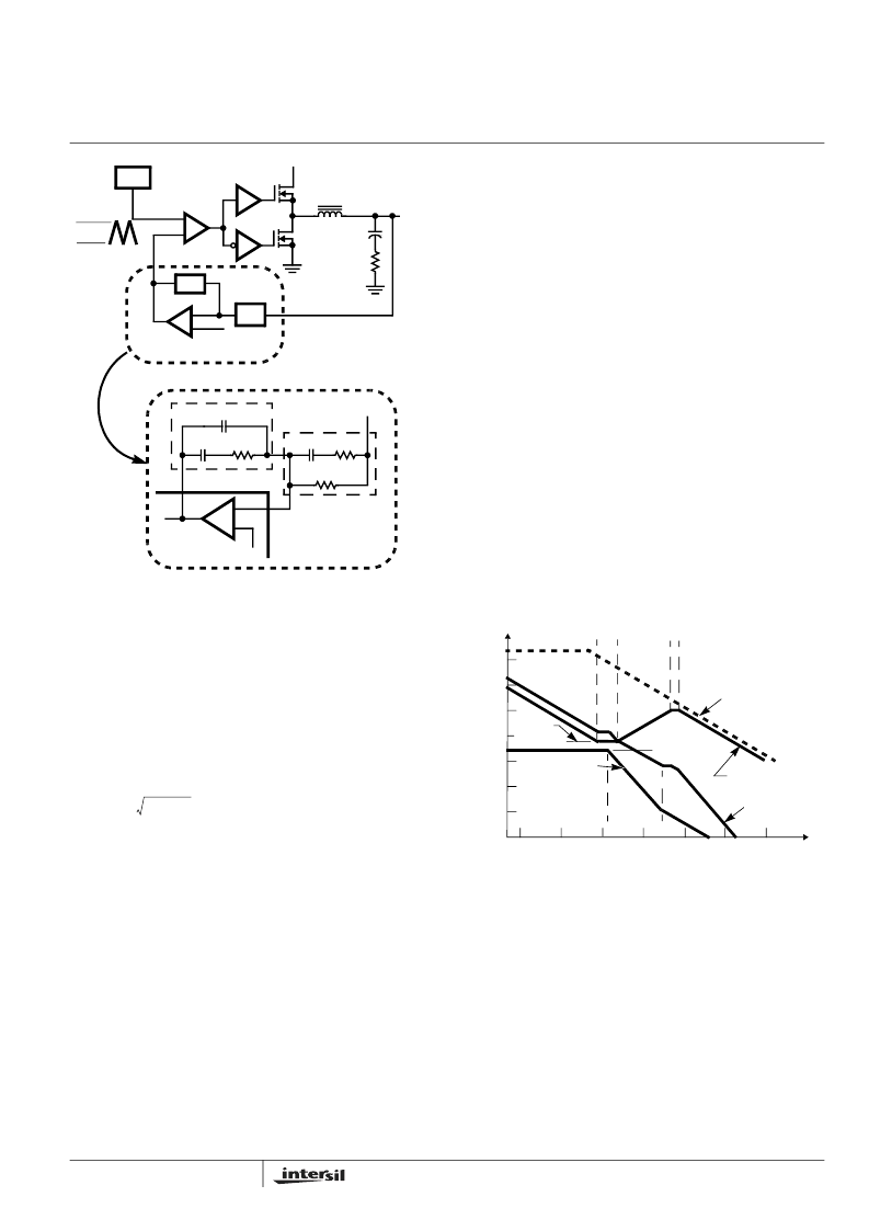
The PWM wave is smoothed by the output filter (L
O
and C
O
).
The modulator transfer function is the small-signal transfer
function of V
OUT
/V
E/A
. This function is dominated by a DC
Gain and the output filter (L
O
and C
O
), with a double pole
break frequency at F
LC
and a zero at F
ESR
. The DC Gain of
the modulator is simply the input voltage (V
IN
) divided by the
peak-to-peak oscillator voltage
V
OSC
.
Modulator Break Frequency Equations
The compensation network consists of the error amplifier
(internal to the HIP6004E) and the impedance networks Z
IN
and Z
FB
. The goal of the compensation network is to provide
a closed loop transfer function with the highest 0dB crossing
frequency (f
0dB
) and adequate phase margin. Phase margin
is the difference between the closed loop phase at f
0dB
and
180
degrees
.
The equations below relate the compensation
network’s poles, zeros and gain to the components (R
1
, R
2
,
R
3
, C
1
, C
2
, and C
3
) in Figure 7. Use these guidelines for
locating the poles and zeros of the compensation network:
1. Pick Gain (R
2
/R
1
) for desired converter bandwidth.
2. Place 1
ST
Zero Below Filter’s Double Pole (~75% F
LC
).
3. Place 2
ND
Zero at Filter’s Double Pole.
4. Place 1
ST
Pole at the ESR Zero.
5. Place 2
ND
Pole at Half the Switching Frequency.
6. Check Gain against Error Amplifier’s Open-Loop Gain.
7. Estimate Phase Margin - Repeat if Necessary.
Compensation Break Frequency Equations
Figure 8 shows an asymptotic plot of the DC-DC converter’s
gain vs. frequency. The actual Modulator Gain has a high gain
peak due to the high Q factor of the output filter and is not
shown in Figure 8. Using the above guidelines should give a
Compensation Gain similar to the curve plotted. The open
loop error amplifier gain bounds the compensation gain.
Check the compensation gain at F
P2
with the capabilities of
the error amplifier. The Closed Loop Gain is constructed on
the log-log graph of Figure 8 by adding the Modulator Gain (in
dB) to the Compensation Gain (in dB). This is equivalent to
multiplying the modulator transfer function to the
compensation transfer function and plotting the gain.
The compensation gain uses external impedance networks
Z
FB
and Z
IN
to provide a stable, high bandwidth (BW) overall
loop. A stable control loop has a gain crossing with
-20dB/decade slope and a phase margin greater than 45
degrees. Include worst case component variations when
determining phase margin.
Component Selection Guidelines
Output Capacitor Selection
An output capacitor is required to filter the output and supply
the load transient current. The filtering requirements are a
function of the switching frequency and the ripple current.
The load transient requirements are a function of the slew
rate (di/dt) and the magnitude of the transient load current.
These requirements are generally met with a mix of
capacitors and careful layout.
Modern microprocessors produce transient load rates above
1A/ns. High frequency capacitors initially supply the transient
and slow the current load rate seen by the bulk capacitors.
FIGURE 7. VOLTAGE-MODE BUCK CONVERTER
COMPENSATION DESIGN
V
OUT
REFERENCE
L
O
C
O
ESR
V
IN
V
OSC
ERROR
AMP
PWM
DRIVER
(PARASITIC)
Z
FB
+
-
DACOUT
R
1
R
3
R
2
C
3
C
2
C
1
COMP
V
OUT
FB
Z
FB
HIP6004E
Z
IN
COMPARATOR
DRIVER
DETAILED COMPENSATION COMPONENTS
PHASE
V
E/A
+
-
+
-
Z
IN
OSC
FLC
2
π
x LO x CO
------------------------------------------
=
FESR
-------------------------------------------
=
F
Z1
2
1
------------------------------------
=
F
Z2
+
2
π
x R
1
R
3
(
)
x C
3
------------------------------------------------------
=
F
P1
2
π
x R
2
x
2
1
C
2
+
---------------------
--------------------------------------------------------
=
F
P2
3
3
------------------------------------
=
100
80
60
40
20
0
-20
-40
-60
F
P1
F
Z2
10M
1M
100K
10K
1K
100
10
OPEN LOOP
ERROR AMP GAIN
F
Z1
F
P2
20LOG
(R
2
/R
1
)
F
LC
F
ESR
COMPENSATION
GAIN
CLOSED LOOP
GAIN
G
FREQUENCY (Hz)
20LOG
(V
IN
/
V
OSC
)
MODULATOR
GAIN
FIGURE 8. ASYMPTOTIC BODE PLOT OF CONVERTER GAIN
HIP6004E
相关PDF资料 |
PDF描述 |
|---|---|
| HIP6004E | Buck and Synchronous-Rectifier (PWM) Controller and Output Voltage Monitor |
| HIP6004ECB | Buck and Synchronous-Rectifier (PWM) Controller and Output Voltage Monitor |
| HIP6004ECV | Buck and Synchronous-Rectifier (PWM) Controller and Output Voltage Monitor |
| HIP6013 | FPGA - 100000 SYSTEM GATE 2.5 VOLT - NOT RECOMMENDED for NEW DESIGN |
| HIP6013CB | FPGA - 100000 SYSTEM GATE 2.5 VOLT - NOT RECOMMENDED for NEW DESIGN |
相关代理商/技术参数 |
参数描述 |
|---|---|
| HIP6004ECVZ-T | 功能描述:电压模式 PWM 控制器 20LD BUCK&SYNCHCT PWMCONOUTPUT RoHS:否 制造商:Texas Instruments 输出端数量:1 拓扑结构:Buck 输出电压:34 V 输出电流: 开关频率: 工作电源电压:4.5 V to 5.5 V 电源电流:600 uA 最大工作温度:+ 125 C 最小工作温度:- 40 C 封装 / 箱体:WSON-8 封装:Reel |
| HIP6004EVAL1 | 功能描述:EVALUATION BOARD HIP6004 RoHS:否 类别:编程器,开发系统 >> 过时/停产零件编号 系列:- 标准包装:1 系列:- 传感器类型:CMOS 成像,彩色(RGB) 传感范围:WVGA 接口:I²C 灵敏度:60 fps 电源电压:5.7 V ~ 6.3 V 嵌入式:否 已供物品:成像器板 已用 IC / 零件:KAC-00401 相关产品:4H2099-ND - SENSOR IMAGE WVGA COLOR 48-PQFP4H2094-ND - SENSOR IMAGE WVGA MONO 48-PQFP |
| HIP6004EVAL3 | 功能描述:电源管理IC开发工具 EMBEDDED EVAL BRD SYNC BUCK/KLAM RoHS:否 制造商:Maxim Integrated 产品:Evaluation Kits 类型:Battery Management 工具用于评估:MAX17710GB 输入电压: 输出电压:1.8 V |
| HIP6005 | 制造商:INTERSIL 制造商全称:Intersil Corporation 功能描述:Buck Pulse-Width Modulator (PWM) Controller and Output Voltage Monitor |
| HIP6005A | 制造商:INTERSIL 制造商全称:Intersil Corporation 功能描述:Buck Pulse-Width Modulator (PWM) Controller and Output Voltage Monitor |
发布紧急采购,3分钟左右您将得到回复。