参数资料
| 型号: | HIP6006CV |
| 厂商: | Intersil |
| 文件页数: | 6/12页 |
| 文件大小: | 0K |
| 描述: | IC CTRLR PWM VOLT MODE 14-TSSOP |
| 标准包装: | 96 |
| 应用: | 控制器,Intel Pentium? Pro、PowerP、Alpha |
| 输入电压: | 5V,12V |
| 输出数: | 1 |
| 输出电压: | 1.3 V ~ 12 V |
| 工作温度: | 0°C ~ 70°C |
| 安装类型: | * |
| 封装/外壳: | 14-TSSOP(0.173",4.40mm 宽) |
| 供应商设备封装: | * |
| 包装: | 管件 |
�� �
�
�HIP6006�
�complete� its� cycle.� Figure� 4� shows� this� operation� with� an�
�overload� condition.� Note� that� the� inductor� current� increases�
�to� over� 15A� during� the� C� SS� charging� interval� and� causes� an�
�over-current� trip.� The� converter� dissipates� very� little� power�
�with� this� method.� The� measured� input� power� for� the�
�HIP6006�
�V� IN�
�conditions� of� Figure� 4� is� 2.5W.�
�The� over-current� function� will� trip� at� a� peak� inductor� current�
�UGATE�
�PHASE�
�Q1�
�L� O�
�V� OUT�
�I� PEAK� =� ---------------------------------------------------�
�(I� PEAK)� determined� by:�
�I� OCSET� ?� R� OCSET�
�r� DS� (� ON� )�
�LGATE�
�PGND�
�Q2�
�D2�
�C� IN�
�C� O�
�3.� Determine� I� PEAK� for� I� PEAK� >� I� OUT� (� MAX� )� +� (� ?� I� )� ?� 2�
�+V� IN�
�L� O�
�C� BOOT�
�HIP6006�
�where� I� OCSET� is� the� internal� OCSET� current� source� (200� μ� A�
�-� typical).� The� OC� trip� point� varies� mainly� due� to� the�
�MOSFETs� r� DS(ON)� variations.� To� avoid� over-current� tripping�
�in� the� normal� operating� load� range,� find� the� R� OCSET� resistor�
�from� the� equation� above� with:�
�1.� The� maximum� r� DS(ON)� at� the� highest� junction�
�temperature.�
�2.� The� minimum� I� OCSET� from� the� specification� table.�
�,�
�where� ?� I� is� the� output� inductor� ripple� current.�
�For� an� equation� for� the� ripple� current� see� the� section� under�
�component� guidelines� titled� ‘Output� Inductor� Selection’.�
�A� small� ceramic� capacitor� should� be� placed� in� parallel� with�
�RETURN�
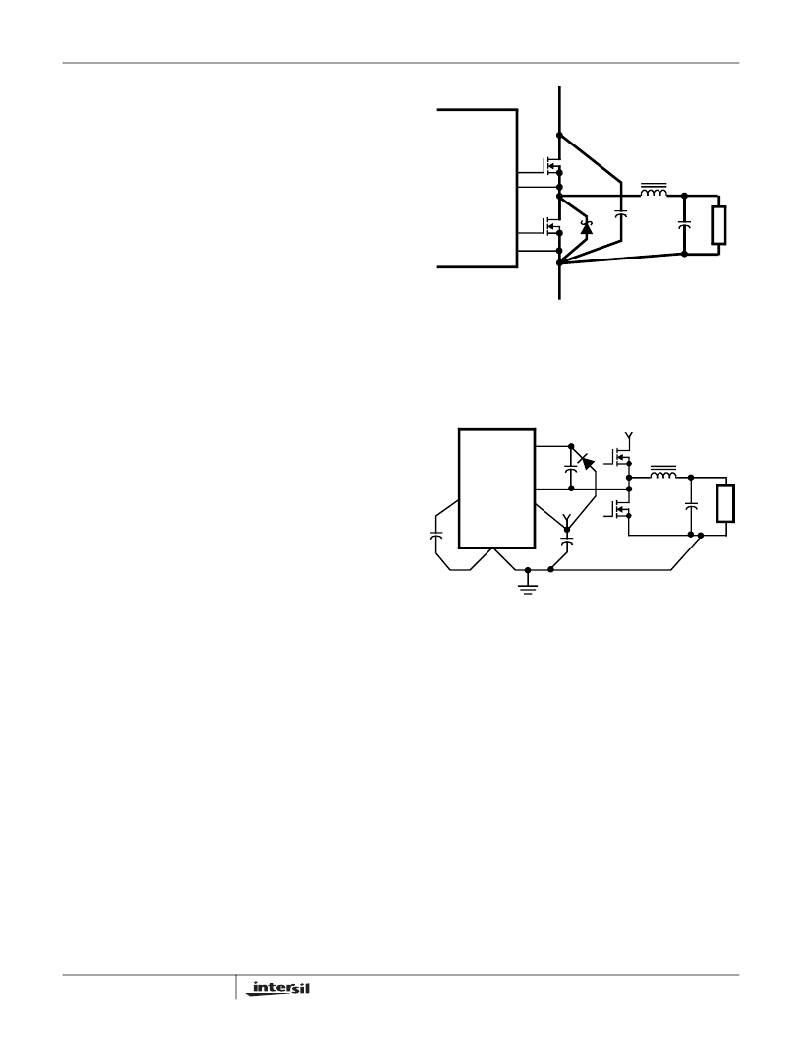
�FIGURE� 5.� PRINTED� CIRCUIT� BOARD� POWER� AND�
�GROUND� PLANES� OR� ISLANDS�
�current� paths� on� the� SS� PIN� and� locate� the� capacitor,� C� ss�
�close� to� the� SS� pin� because� the� internal� current� source� is�
�only� 10� μ� A.� Provide� local� V� CC� decoupling� between� VCC� and�
�GND� pins.� Locate� the� capacitor,� C� BOOT� as� close� as� practical�
�to� the� BOOT� and� PHASE� pins.�
�BOOT�
�D1�
�Q1�
�V� OUT�
�PHASE�
�R� OCSET� to� smooth� the� voltage� across� R� OCSET� in� the�
�presence� of� switching� noise� on� the� input� voltage.�
�SS�
�+12V�
�Q2�
�C� O�
�VCC�
�Application� Guidelines�
�Layout� Considerations�
�As� in� any� high� frequency� switching� converter,� layout� is� very�
�C� SS�
�GND�
�C� VCC�
�important.� Switching� current� from� one� power� device� to�
�another� can� generate� voltage� transients� across� the�
�impedances� of� the� interconnecting� bond� wires� and� circuit�
�traces.� These� interconnecting� impedances� should� be�
�minimized� by� using� wide,� short� printed� circuit� traces.� The�
�critical� components� should� be� located� as� close� together� as�
�possible� using� ground� plane� construction� or� single� point�
�grounding.�
�Figure� 5� shows� the� critical� power� components� of� the�
�converter.� To� minimize� the� voltage� overshoot� the�
�interconnecting� wires� indicated� by� heavy� lines� should� be� part�
�of� ground� or� power� plane� in� a� printed� circuit� board.� The�
�components� shown� in� Figure� 6� should� be� located� as� close�
�together� as� possible.� Please� note� that� the� capacitors� C� IN�
�and� C� O� each� represent� numerous� physical� capacitors.�
�Locate� the� HIP6006� within� 3� inches� of� the� MOSFETs,� Q1�
�and� Q2.� The� circuit� traces� for� the� MOSFETs’� gate� and�
�source� connections� from� the� HIP6006� must� be� sized� to�
�handle� up� to� 1A� peak� current.�
�Figure� 6� shows� the� circuit� traces� that� require� additional�
�layout� consideration.� Use� single� point� and� ground� plane�
�construction� for� the� circuits� shown.� Minimize� any� leakage�
�6�
�FIGURE� 6.� PRINTED� CIRCUIT� BOARD� SMALL� SIGNAL�
�LAYOUT� GUIDELINES�
�Feedback� Compensation�
�Figure� 7� highlights� the� voltage-mode� control� loop� for� a�
�synchronous-rectified� buck� converter.� The� output� voltage�
�(Vout)� is� regulated� to� the� Reference� voltage� level.� The� error�
�amplifier� (Error� Amp)� output� (V� E/A� )� is� compared� with� the�
�oscillator� (OSC)� triangular� wave� to� provide� a� pulse-width�
�modulated� (PWM)� wave� with� an� amplitude� of� V� IN� at� the�
�PHASE� node.� The� PWM� wave� is� smoothed� by� the� output� filter�
�(L� O� and� C� O� ).�
�The� modulator� transfer� function� is� the� small-signal� transfer�
�function� of� Vout/V� E/A� .� This� function� is� dominated� by� a� DC�
�Gain� and� the� output� filter� (L� O� and� C� O� ),� with� a� double� pole�
�break� frequency� at� F� LC� and� a� zero� at� F� ESR� .� The� DC� Gain� of�
�the� modulator� is� simply� the� input� voltage� (V� IN� )� divided� by� the�
�peak-to-peak� oscillator� voltage� ?� V� OSC� .�
�相关PDF资料 |
PDF描述 |
|---|---|
| HIP6006CB | IC CTRLR PWM VOLTAGE MODE 14SOIC |
| UWZ0J152MCL1GS | CAP ALUM 1500UF 6.3V 20% SMD |
| HIP6004ECV | IC CTRLR PWM VOLTAGE MON 20TSSOP |
| HIP6004BCB | IC CTRLR PWM VOLTAGE MON 20-SOIC |
| UVK2V3R3MPD | CAP ALUM 3.3UF 350V 20% RADIAL |
相关代理商/技术参数 |
参数描述 |
|---|---|
| HIP6006CV-T | 功能描述:IC CTRLR PWM VOLT MODE 14-TSSOP RoHS:否 类别:集成电路 (IC) >> PMIC - 稳压器 - 专用型 系列:- 产品培训模块:Lead (SnPb) Finish for COTS Obsolescence Mitigation Program 标准包装:2,000 系列:- 应用:电源,ICERA E400,E450 输入电压:4.1 V ~ 5.5 V 输出数:10 输出电压:可编程 工作温度:-40°C ~ 85°C 安装类型:表面贴装 封装/外壳:42-WFBGA,WLCSP 供应商设备封装:42-WLP 包装:带卷 (TR) |
| HIP6006CV-TS2462 | 制造商:Rochester Electronics LLC 功能描述:- Bulk |
| HIP6006EVAL1 | 功能描述:电源管理IC开发工具 SYNC BUCK EVAL BRD RoHS:否 制造商:Maxim Integrated 产品:Evaluation Kits 类型:Battery Management 工具用于评估:MAX17710GB 输入电压: 输出电压:1.8 V |
| HIP6007 | 制造商:INTERSIL 制造商全称:Intersil Corporation 功能描述:Buck Pulse-Width Modulator (PWM) Controller |
| HIP6007CB | 功能描述:IC CTRLR PWM STD BUCK 14-SOIC RoHS:否 类别:集成电路 (IC) >> PMIC - 稳压器 - 专用型 系列:- 产品培训模块:Lead (SnPb) Finish for COTS Obsolescence Mitigation Program 标准包装:2,000 系列:- 应用:电源,ICERA E400,E450 输入电压:4.1 V ~ 5.5 V 输出数:10 输出电压:可编程 工作温度:-40°C ~ 85°C 安装类型:表面贴装 封装/外壳:42-WFBGA,WLCSP 供应商设备封装:42-WLP 包装:带卷 (TR) |
发布紧急采购,3分钟左右您将得到回复。