参数资料
| 型号: | HIP6007CB |
| 厂商: | Intersil |
| 文件页数: | 9/10页 |
| 文件大小: | 0K |
| 描述: | IC CTRLR PWM STD BUCK 14-SOIC |
| 标准包装: | 50 |
| 应用: | 控制器,Intel Pentium? Pro、PowerP、Alpha |
| 输入电压: | 2.5 V ~ 12 V |
| 输出数: | 1 |
| 输出电压: | 1.27 V ~ 12 V |
| 工作温度: | 0°C ~ 70°C |
| 安装类型: | 表面贴装 |
| 封装/外壳: | 14-SOIC(0.154",3.90mm 宽) |
| 供应商设备封装: | 14-SOICN |
| 包装: | 管件 |
�� �
�
�HIP6007�
�MOSFET� Selection/Considerations�
�The� HIP6007� requires� an� N-Channel� power� MOSFET.� It�
�+12V�
�D� BOOT�
�should� be� selected� based� upon� r� DS(ON)� ,� gate� supply�
�requirements,� and� thermal� management� requirements.�
�VCC�
�+�
�V� D�
�-�
�+5V� OR� +12V�
�In� high-current� applications,� the� MOSFET� power�
�dissipation,� package� selection� and� heatsink� are� the�
�dominant� design� factors.� The� power� dissipation� includes�
�two� loss� components;� conduction� loss� and� switching� loss.�
�HIP6007�
�BOOT�
�UGATE�
�PHASE�
�C� BOOT�
�Q1�
�NOTE:�
�V� G-S� ≈� V� CC� -� V� D�
�The� conduction� losses� are� the� largest� component� of� power�
�dissipation� for� the� MOSFET.� Switching� losses� also�
�contribute� to� the� overall� MOSFET� power� loss� (see� the�
�equations� below).� These� equations� assume� linear� voltage-�
�current� transitions� and� are� approximations.� The� gate-�
�charge� losses� are� dissipated� by� the� HIP6007� and� don't�
�heat� the� MOSFET.� However,� large� gate-charge� increases�
�the� switching� interval,� t� SW� ,� which� increases� the� upper�
�MOSFET� switching� losses.� Ensure� that� the� MOSFET� is�
�within� its� maximum� junction� temperature� at� high� ambient�
�D2�
�-�
�+�
�GND�
�FIGURE� 9.� UPPER� GATE� DRIVE� -� BOOTSTRAP� OPTION�
�temperature� by� calculating� the� temperature� rise� according�
�to� package� thermal-resistance� specifications.� A� separate�
�heatsink� may� be� necessary� depending� upon� MOSFET�
�+12V�
�VCC�
�+5V� OR� LESS�
�P� SW� =� 2� I� O� x� V� IN� x� t� SW� x� Fs�
�power,� package� type,� ambient� temperature� and� air� flow.�
�P� COND� =� I� O2� x� r� DS(ON)� x� D�
�1�
�Where:� D� is� the� duty� cycle� =� V� O� /� V� IN� ,�
�t� SW� is� the� switching� interval,� and�
�Fs� is� the� switching� frequency.�
�HIP6007�
�-�
�+�
�BOOT�
�UGATE�
�PHASE�
�Q1�
�D2�
�NOTE:�
�V� G-S� ≈� V� CC� -� 5V�
�Standard-gate� MOSFETs� are� normally� recommended� for�
�use� with� the� HIP6007.� However,� logic-level� gate� MOSFETs�
�can� be� used� under� special� circumstances.� The� input� voltage,�
�upper� gate� drive� level,� and� the� MOSFET’s� absolute� gate-to-�
�source� voltage� rating� determine� whether� logic-level�
�MOSFETs� are� appropriate.�
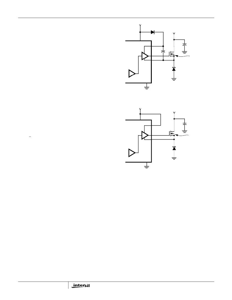
�Figure� 9� shows� the� upper� gate� drive� (BOOT� pin)� supplied� by�
�a� bootstrap� circuit� from� V� CC� .� The� boot� capacitor,� C� BOOT�
�develops� a� floating� supply� voltage� referenced� to� the� PHASE�
�pin.� This� supply� is� refreshed� each� cycle� to� a� voltage� of� V� CC�
�less� the� boot� diode� drop� (V� D� )� when� the� lower� MOSFET,� Q2�
�turns� on.� A� logic-level� MOSFET� can� only� be� used� for� Q1� if�
�the� MOSFET’s� absolute� gate-to-source� voltage� rating�
�exceeds� the� maximum� voltage� applied� to� V� CC� .�
�Figure� 10� shows� the� upper� gate� drive� supplied� by� a� direct�
�connection� to� VCC.� This� option� should� only� be� used� in�
�converter� systems� where� the� main� input� voltage� is� +5VDC�
�or� less.� The� peak� upper� gate-to-source� voltage� is�
�approximately� V� CC� less� the� input� supply.� For� +5V� main�
�power� and� +12VDC� for� the� bias,� the� gate-to-source� voltage�
�of� Q1� is� 7V.� A� logic-level� MOSFET� is� a� good� choice� for� Q1�
�and� a� logic-level� MOSFET� is� a� good� choice� for� Q1� under�
�these� conditions.�
�139�
�GND�
�FIGURE� 10.� UPPER� GATE� DRIVE� -� DIRECT� V� CC� DRIVE� OPTION�
�Schottky� Selection�
�Rectifier� D2� conducts� when� the� upper� MOSFET� Q1� is� off.�
�The� diode� should� be� a� Schottky� type� for� low� power� losses.�
�The� power� dissipation� in� the� schottky� rectifier� is�
�approximated� by:�
�P� COND� =� I� O� x� V� f� x� (1� -� D)�
�Where:� D� is� the� duty� cycle� =� V� O� /V� IN� ,� and�
�V� f� is� the� schottky� forward� voltage� drop�
�In� addition� to� power� dissipation,� package� selection� and�
�heatsink� requirements� are� the� main� design� tradeoffs� in�
�choosing� the� schottky� rectifier.� Since� the� three� factors� are�
�interrelated,� the� selection� process� is� an� iterative� procedure.�
�The� maximum� junction� temperature� of� the� rectifier� must�
�remain� below� the� manufacturer’s� specified� value,� typically�
�125� o� C.� By� using� the� package� thermal� resistance� specification�
�and� the� schottky� power� dissipation� equation� (shown� above),�
�the� junction� temperature� of� the� rectifier� can� be� estimated.� Be�
�sure� to� use� the� available� airflow� and� ambient� temperature� to�
�determine� the� junction� temperature� rise.�
�相关PDF资料 |
PDF描述 |
|---|---|
| SDS850R-183M | INDUCTOR PWR SHIELDED 18UH SMD |
| MCP1700T-2602E/TT | IC REG LDO 2.6V .25A SOT-23-3 |
| HIP6006CV | IC CTRLR PWM VOLT MODE 14-TSSOP |
| HIP6006CB | IC CTRLR PWM VOLTAGE MODE 14SOIC |
| UWZ0J152MCL1GS | CAP ALUM 1500UF 6.3V 20% SMD |
相关代理商/技术参数 |
参数描述 |
|---|---|
| HIP6007CB-T | 功能描述:IC CTRLR PWM STD BUCK 14-SOIC RoHS:否 类别:集成电路 (IC) >> PMIC - 稳压器 - 专用型 系列:- 产品培训模块:Lead (SnPb) Finish for COTS Obsolescence Mitigation Program 标准包装:2,000 系列:- 应用:电源,ICERA E400,E450 输入电压:4.1 V ~ 5.5 V 输出数:10 输出电压:可编程 工作温度:-40°C ~ 85°C 安装类型:表面贴装 封装/外壳:42-WFBGA,WLCSP 供应商设备封装:42-WLP 包装:带卷 (TR) |
| HIP6007EVAL1 | 制造商:Intersil Corporation 功能描述:EVAL KIT FOR BUCK PULSE-WIDTH MODULATOR (PWM) CNTRLR - Bulk |
| HIP6008 | 制造商:INTERSIL 制造商全称:Intersil Corporation 功能描述:Buck Pulse-Width Modulator (PWM) Controller and Output Voltage Monitor |
| HIP6008CB | 制造商:Rochester Electronics LLC 功能描述:PWMCONTROLLER4/BITDACW/4BITDAC1.5%16NBSOIC" - Bulk |
| HIP6008CB-T | 制造商:Rochester Electronics LLC 功能描述:- Bulk |
发布紧急采购,3分钟左右您将得到回复。