- 您现在的位置:买卖IC网 > PDF目录13161 > HIP6012CBZ-T (Intersil)IC CTRLR PWM BUCK SYNC 14-SOIC PDF资料下载
参数资料
| 型号: | HIP6012CBZ-T |
| 厂商: | Intersil |
| 文件页数: | 9/12页 |
| 文件大小: | 0K |
| 描述: | IC CTRLR PWM BUCK SYNC 14-SOIC |
| 标准包装: | 1 |
| 应用: | 控制器,Intel Pentium? Pro、PowerP、Alpha |
| 输入电压: | 5V,12V |
| 输出数: | 1 |
| 输出电压: | 1.3 V ~ 12 V |
| 工作温度: | 0°C ~ 70°C |
| 安装类型: | * |
| 封装/外壳: | 14-SOIC(0.154",3.90mm 宽) |
| 供应商设备封装: | * |
| 包装: | 标准包装 |
| 产品目录页面: | 1242 (CN2011-ZH PDF) |
| 其它名称: | HIP6012CBZ-TDKR |
�� �
�
�HIP6012�
�These� equations� assume� linear� voltage-current� transitions�
�and� do� not� adequately� model� power� loss� due� the� reverse-�
�recovery� of� the� lower� MOSFETs� body� diode.� The�
�gate-charge� losses� are� dissipated� by� the� HIP6012� and� don't�
�heat� the� MOSFETs.� However,� large� gate-charge� increases�
�the� switching� interval,� t� SW� which� increases� the� upper�
�MOSFET� switching� losses.� Ensure� that� both� MOSFETs� are�
�within� their� maximum� junction� temperature� at� high� ambient�
�temperature� by� calculating� the� temperature� rise� according� to�
�package� thermal-resistance� specifications.� A� separate�
�heatsink� may� be� necessary� depending� upon� MOSFET�
�power,� package� type,� ambient� temperature� and� air� flow.�
�Standard-gate� MOSFETs� are� normally� recommended� for�
�use� with� the� HIP6012.� However,� logic-level� gate� MOSFETs�
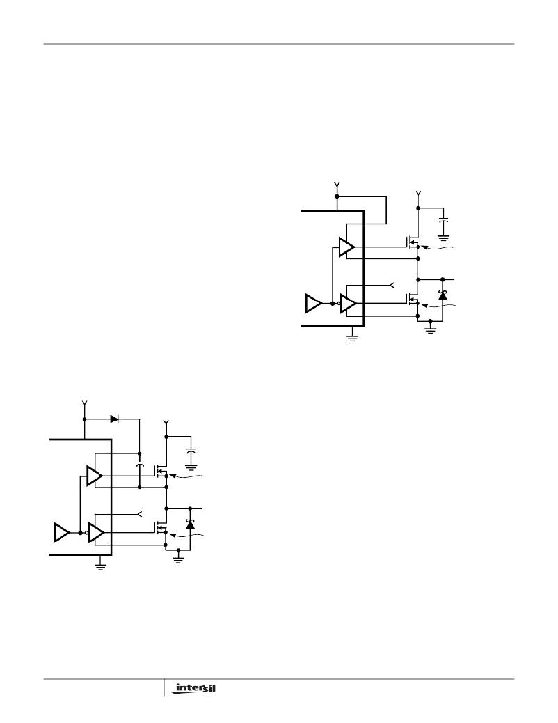
�Figure� 10� shows� the� upper� gate� drive� supplied� by� a� direct�
�connection� to� V� CC� .� This� option� should� only� be� used� in�
�converter� systems� where� the� main� input� voltage� is� +5� VDC�
�or� less.� The� peak� upper� gate-to-source� voltage� is�
�approximately� VCC� less� the� input� supply.� For� +5V� main�
�power� and� +12� VDC� for� the� bias,� the� gate-to-source� voltage�
�of� Q1� is� 7V.� A� logic-level� MOSFET� is� a� good� choice� for� Q1�
�and� a� logic-level� MOSFET� can� be� used� for� Q2� if� its� absolute�
�gate-to-source� voltage� rating� exceeds� the� maximum� voltage�
�applied� to� PVCC.�
�+12V�
�+5V� OR� LESS�
�VCC�
�can� be� used� under� special� circumstances.� The� input� voltage,�
�upper� gate� drive� level,� and� the� MOSFETs� absolute� gate-to-�
�HIP6012�
�BOOT�
�source� voltage� rating� determine� whether� logic-level�
�MOSFETs� are� appropriate.�
�Figure� 9� shows� the� upper� gate� drive� (BOOT� pin)� supplied� by�
�a� bootstrap� circuit� from� V� CC� .� The� boot� capacitor,� C� BOOT�
�UGATE�
�PHASE�
�+5V�
�OR� +12V�
�PVCC�
�Q1�
�NOTE:�
�V� G-S� ≈� V� CC� -� 5V�
�develops� a� floating� supply� voltage� referenced� to� the� PHASE�
�pin.� This� supply� is� refreshed� each� cycle� to� a� voltage� of� V� CC�
�less� the� boot� diode� drop� (V� D� )� when� the� lower� MOSFET,� Q2�
�-�
�+�
�LGATE�
�PGND�
�Q2�
�D2�
�NOTE:�
�V� G-S� ≈� PVCC�
�turns� on.� A� logic-level� MOSFET� can� only� be� used� for� Q1� if�
�the� MOSFETs� absolute� gate-to-source� voltage� rating�
�exceeds� the� maximum� voltage� applied� to� V� CC� .� For� Q2,� a�
�logic-level� MOSFET� can� be� used� if� its� absolute� gate-to-�
�source� voltage� rating� exceeds� the� maximum� voltage� applied�
�to� PVCC.�
�GND�
�FIGURE� 10.� UPPER� GATE� DRIVE� -� DIRECT� V� CC� DRIVE� OPTION�
�Schottky� Selection�
�+12V�
�D� BOOT�
�Rectifier� D2� is� a� clamp� that� catches� the� negative� inductor�
�swing� during� the� dead� time� between� turning� off� the� lower�
�VCC�
�+�
�VO�
�-�
�+5V� OR� +12V�
�MOSFET� and� turning� on� the� upper� MOSFET.� The� diode� must�
�be� a� Schottky� type� to� prevent� the� lossy� parasitic� MOSFET�
�body� diode� from� conducting.� It� is� acceptable� to� omit� the� diode�
�HIP6012�
�BOOT�
�UGATE�
�PHASE�
�C� BOOT�
�Q1�
�NOTE:�
�V� G-S� ≈� V� CC� -� V� D�
�and� let� the� body� diode� of� the� lower� MOSFET� clamp� the�
�negative� inductor� swing,� but� efficiency� will� drop� one� or� two�
�percent� as� a� result.� The� diode's� rated� reverse� breakdown�
�voltage� must� be� greater� than� the� maximum� input� voltage.�
�+5V�
�PVCC� OR� +12V�
�-�
�+�
�LGATE�
�PGND�
�Q2�
�D2�
�NOTE:�
�V� G-S� ≈� PVCC�
�GND�
�FIGURE� 9.� UPPER� GATE� DRIVE� -� BOOTSTRAP� OPTION�
�9�
�FN4324.2�
�December� 27,� 2004�
�相关PDF资料 |
PDF描述 |
|---|---|
| RYM24DTBT-S189 | CONN EDGECARD 48POS R/A .156 SLD |
| VE-BNW-EU | CONVERTER MOD DC/DC 5.5V 200W |
| MIC2774L-44BM5 TR | IC SUPERVISOR DUAL LV SOT23-5 |
| ISL6314CRZ | IC CTRLR PWM 1PHASE BUCK 32-QFN |
| VE-BNV-EU | CONVERTER MOD DC/DC 5.8V 200W |
相关代理商/技术参数 |
参数描述 |
|---|---|
| HIP6012CV | 功能描述:IC CTRLR PWM SYNC BUCK 14-TSSOP RoHS:否 类别:集成电路 (IC) >> PMIC - 稳压器 - 专用型 系列:- 产品培训模块:Lead (SnPb) Finish for COTS Obsolescence Mitigation Program 标准包装:2,000 系列:- 应用:电源,ICERA E400,E450 输入电压:4.1 V ~ 5.5 V 输出数:10 输出电压:可编程 工作温度:-40°C ~ 85°C 安装类型:表面贴装 封装/外壳:42-WFBGA,WLCSP 供应商设备封装:42-WLP 包装:带卷 (TR) |
| HIP6012CV-T | 功能描述:IC CTRLR PWM SYNC BUCK 14-TSSOP RoHS:否 类别:集成电路 (IC) >> PMIC - 稳压器 - 专用型 系列:- 产品培训模块:Lead (SnPb) Finish for COTS Obsolescence Mitigation Program 标准包装:2,000 系列:- 应用:电源,ICERA E400,E450 输入电压:4.1 V ~ 5.5 V 输出数:10 输出电压:可编程 工作温度:-40°C ~ 85°C 安装类型:表面贴装 封装/外壳:42-WFBGA,WLCSP 供应商设备封装:42-WLP 包装:带卷 (TR) |
| HIP6012CVZ | 制造商:INTERSIL 制造商全称:Intersil Corporation 功能描述:Buck and Synchronous-Rectifier Pulse-Width Modulator (PWM) Controller |
| HIP6012EVAL1 | 功能描述:电源管理IC开发工具 DISK DRIVE SUPPLY EVAL BRD RoHS:否 制造商:Maxim Integrated 产品:Evaluation Kits 类型:Battery Management 工具用于评估:MAX17710GB 输入电压: 输出电压:1.8 V |
| HIP6013 | 制造商:INTERSIL 制造商全称:Intersil Corporation 功能描述:Buck Pulse-Width Modulator (PWM) Controller |
发布紧急采购,3分钟左右您将得到回复。