- 您现在的位置:买卖IC网 > PDF目录385382 > HIP6014CB (INTERSIL CORP) Buck and Synchronous-Rectifier (PWM) Controller and Output Voltage Monitor PDF资料下载
参数资料
| 型号: | HIP6014CB |
| 厂商: | INTERSIL CORP |
| 元件分类: | 稳压器 |
| 英文描述: | Buck and Synchronous-Rectifier (PWM) Controller and Output Voltage Monitor |
| 中文描述: | 0.5 A SWITCHING CONTROLLER, 1000 kHz SWITCHING FREQ-MAX, PDSO20 |
| 封装: | PLASTIC, MS-013AC, SOIC-20 |
| 文件页数: | 8/12页 |
| 文件大小: | 211K |
| 代理商: | HIP6014CB |
8
The modulator transfer function is the small-signal transfer
function of V
OUT
/V
E/A
. This function is dominated by a DC
Gain and the output filter (L
O
and C
O
), with a double pole
break frequency at F
LC
and a zero at F
ESR
. The DC Gain of
the modulator is simply the input voltage (V
IN
) divided by the
peak-to-peak oscillator voltage
V
OSC
.
Modulator Break Frequency Equations
The compensation network consists of the error amplifier
(internal to the HIP6014) and the impedance networks Z
IN
and Z
FB
. The goal of the compensation network is to provide
a closed loop transfer function with the highest 0dB crossing
frequency (f
0dB
) and adequate phase margin. Phase margin
is the difference between the closed loop phase at f
0dB
and
180 degrees
.
The equations below relate the compensation
network’s poles, zeros and gain to the components (R
1
, R
2
,
R
3
, C
1
, C
2
, and C
3
) in Figure 7. Use these guidelines for
locating the poles and zeros of the compensation network:
1. Pick Gain (R
2
/R
1
) for desired converter bandwidth
2. Place 1
ST
Zero Below Filter’s Double Pole (~75% F
LC
)
3. Place 2
ND
Zero at Filter’s Double Pole
4. Place 1
ST
Pole at the ESR Zero
5. Place 2
ND
Pole at Half the Switching Frequency
6. Check Gain against Error Amplifier’s Open-Loop Gain
7. Estimate Phase Margin - Repeat if Necessary
Compensation Break Frequency Equations
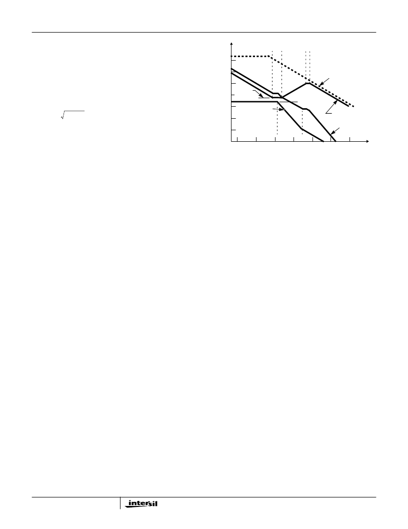
Figure 8 shows an asymptotic plot of the DC-DC converter’s
gain vs. frequency. The actual Modulator Gain has a high gain
peak due to the high Q factor of the output filter and is not
shown in Figure 8. Using the above guidelines should give a
Compensation Gain similar to the curve plotted. The open
loop error amplifier gain bounds the compensation gain.
Check the compensation gain at F
P2
with the capabilities of
the error amplifier. The Closed Loop Gain is constructed on
the log-log graph of Figure 8 by adding the Modulator Gain (in
dB) to the Compensation Gain (in dB). This is equivalent to
multiplying the modulator transfer function to the
compensation transfer function and plotting the gain.
The compensation gain uses external impedance networks
Z
FB
and Z
IN
to provide a stable, high bandwidth (BW) overall
loop. A stable control loop has a gain crossing with
-20dB/decade slope and a phase margin greater than 45
degrees. Include worst case component variations when
determining phase margin.
Component Selection Guidelines
Output Capacitor Selection
An output capacitor is required to filter the output and supply
the load transient current. The filtering requirements are a
function of the switching frequency and the ripple current.
The load transient requirements are a function of the slew
rate (di/dt) and the magnitude of the transient load current.
These requirements are generally met with a mix of
capacitors and careful layout.
Modern microprocessors produce transient load rates
above 1A/ns. High frequency capacitors initially supply the
transient and slow the current load rate seen by the bulk
capacitors. The bulk filter capacitor values are generally
determined by the ESR (effective series resistance) and
voltage rating requirements rather than actual capacitance
requirements.
High frequency decoupling capacitors should be placed as
close to the power pins of the load as physically possible. Be
careful not to add inductance in the circuit board wiring that
could cancel the usefulness of these low inductance
components. Consult with the manufacturer of the load on
specific decoupling requirements. For example, Intel
recommends that the high frequency decoupling for the
Pentium Pro be composed of at least forty (40) 1
μ
F ceramic
capacitors in the 1206 surface-mount package.
Use only specialized low-ESR capacitors intended for
switching-regulator applications for the bulk capacitors. The
bulk capacitor’s ESR will determine the output ripple
voltage and the initial voltage drop after a high slew-rate
transient. An aluminum electrolytic capacitor’s ESR value is
related to the case size with lower ESR available in larger
case sizes. However, the equivalent series inductance
(ESL) of these capacitors increases with case size and can
reduce the usefulness of the capacitor to high slew-rate
transient loading. Unfortunately, ESL is not a specified
parameter. Work with your capacitor supplier and measure
the capacitor’s impedance with frequency to select a
FLC
LO
2
π
CO
---------------------------------------
=
FESR
----------------------------------------
=
F
Z1
2
1
---------------------------------
=
F
Z2
1
R
3
)
C
3
------------------------+
=
F
P1
2
π
R
2
1
2
C
2
+
--------------------
----------------------------------------------------
=
F
P2
3
3
---------------------------------
=
100
80
60
40
20
0
-20
-40
-60
F
P1
F
Z2
10M
1M
100K
10K
1K
100
10
OPEN LOOP
ERROR AMP GAIN
F
Z1
F
P2
20LOG
(R
2
/R
1
)
F
LC
F
ESR
COMPENSATION
GAIN
G
FREQUENCY (Hz)
20LOG
(V
IN
/
V
OSC
)
MODULATOR
GAIN
FIGURE 8. ASYMPTOTIC BODE PLOT OF CONVERTER GAIN
CLOSED LOOP
GAIN
HIP6014
相关PDF资料 |
PDF描述 |
|---|---|
| HIP6016 | FPGA - 100000 SYSTEM GATE 2.5 VOLT - NOT RECOMMENDED for NEW DESIGN |
| HIP6016CB | Advanced PWM and Dual Linear Power Control |
| HIP6017B | FPGA - 100000 SYSTEM GATE 2.5 VOLT - NOT RECOMMENDED for NEW DESIGN |
| HIP6017BCB | FPGA - 100000 SYSTEM GATE 2.5 VOLT - NOT RECOMMENDED for NEW DESIGN |
| HIP6018B | 100,000 System Gate FPGA - NOT RECOMMENDED for NEW DESIGN |
相关代理商/技术参数 |
参数描述 |
|---|---|
| HIP6014CB WAF | 制造商:Harris Corporation 功能描述: |
| HIP6014CB-T | 制造商:Rochester Electronics LLC 功能描述:- Bulk |
| HIP6015 | 制造商:INTERSIL 制造商全称:Intersil Corporation 功能描述:Buck Pulse-Width Modulator (PWM) Controller and Output Voltage Monitor |
| HIP6015 WAF | 制造商:Harris Corporation 功能描述: |
| HIP6015CB | 制造商:Rochester Electronics LLC 功能描述:- Bulk 制造商:Harris Corporation 功能描述: |
发布紧急采购,3分钟左右您将得到回复。