- 您现在的位置:买卖IC网 > PDF目录371821 > HIP6017CB (HARRIS SEMICONDUCTOR) Advanced PWM and Dual Linear Power Control PDF资料下载
参数资料
| 型号: | HIP6017CB |
| 厂商: | HARRIS SEMICONDUCTOR |
| 元件分类: | 稳压器 |
| 英文描述: | Advanced PWM and Dual Linear Power Control |
| 中文描述: | SWITCHING CONTROLLER, 215 kHz SWITCHING FREQ-MAX, PDSO28 |
| 文件页数: | 8/14页 |
| 文件大小: | 135K |
| 代理商: | HIP6017CB |
2-217
allows V
OUT2
and V
OUT3
to slew up without generating a
fault. Cycling the bias input voltage (+12V
IN
on the VCC
pin) off then on resets the counter and the fault latch.
Over-Voltage Protection
During operation, a short on the upper PWM MOSFET (Q1)
causes V
OUT1
to increase. When the output exceeds the
over-voltage threshold of 115% (typical) of DACOUT, the
over-voltage comparator trips to set the fault latch and turns
Q2 on as required in order to regulate V
OUT1
to 1.15 x
DACOUT. This blows the input fuse and reduces V
OUT1
.
The fault latch raises the FAULT/RT pin close to VCC
potential.
A separate over-voltage circuit provides protection during
the initial application of power. For voltages on the VCC pin
below the power-on reset (and above ~4V), V
OUT1
is
monitored for voltages exceeding 1.26V. Should VSEN1
exceed this level, the lower MOSFET (Q2) is driven on as
needed to regulate V
OUT1
to 1.26V.
Over-Current Protection
All outputs are protected against excessive over-currents.
The PWM controller uses the upper MOSFET’s on-
resistance, r
DS(ON)
to monitor the current for protection
against shorted outputs. The linear regulator monitors the
current of the integrated power device and signals an over-
current condition for currents in excess of 230mA.
Additionally, both the linear regulator and the linear controller
monitor FB2 and FB3 for under-voltage to protect against
excessive currents.
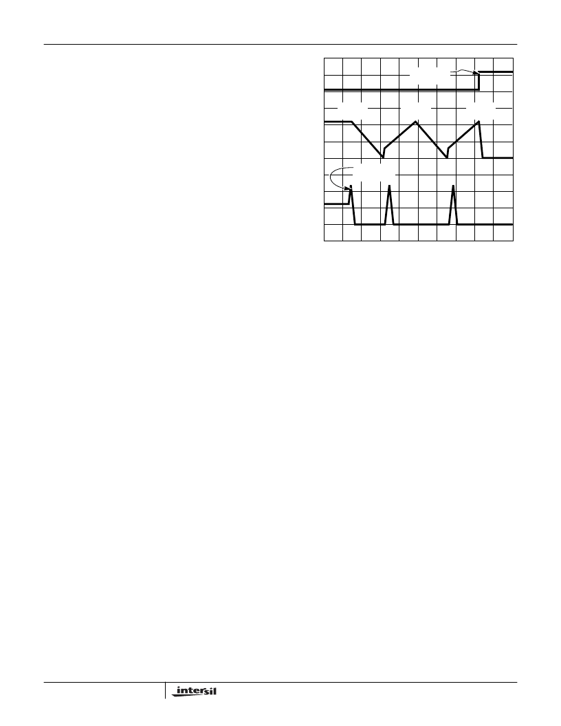
Figures 8 and 9 illustrate the over-current protection with
an overload on OUT1. The overload is applied at T0 and
the current increases through the output inductor (L
OUT1
).
At time T1, the OVER-CURRENT1 comparator trips when
the voltage across Q1 (I
D
r
DS(ON)
) exceeds the level
programmed by R
OCSET
. This inhibits all outputs,
discharges the soft-start capacitor (C
SS
) with a 11mA
current sink, and increments the counter. C
SS
recharges at
T2 and initiates a soft-start cycle with the error amplifiers
clamped by soft-start. With OUT1 still overloaded, the
inductor current increases to trip the over-current
comparator. Again, this inhibits all outputs, but the soft-start
voltage continues increasing to 4V before discharging. The
counter increments to 2. The soft-start cycle repeats at T3
and trips the over-current comparator. The SS pin voltage
increases to 4V at T4 and the counter increments to 3. This
sets the fault latch to disable the converter. The fault is
reported on the FAULT/RT pin.
The linear regulator operates in the same way as PWM1 to
over-current faults. Additionally, the linear regulator and
linear controller monitor the feedback pins for an under-
voltage. Should excessive currents cause FB2 or FB3 to fall
below the linear under-voltage threshold, the LUV signal
sets the over-current latch if C
SS
isfully charged. Blanking the
LUV signal during the C
SS
charge interval allows the linear
outputs to build above the under-voltage threshold during
normal start-up. Cycling the bias input power off then on
resets the counter and the fault latch.
Resistor R
OCSET1
programs the over-current trip level for the
PWM converter. As shown in Figure 9, the internal 200
μ
A
current sink develops a voltage across R
OCSET
(V
SET
) that is
referenced to V
IN
. The DRIVE signal enables the over-current
comparator (OVER-CURRENT1). When the voltage across
the upper MOSFET (V
DS(ON)
) exceeds V
SET
, the over-
current comparator trips to set the over-current latch. Both
V
SET
and V
DS
are referenced to V
IN
and a small capacitor
across R
OCSET
helps V
OCSET
track the variations of V
IN
due
to MOSFET switching. The over-current function will trip at a
peak inductor current (I
PEAK
) determined by:
The OC trip point varies with MOSFET’s temperature. To
avoid over-current tripping in the normal operating load
range, determine the R
OCSET
resistor from the equation
above with:
1. Themaximumr
DS(ON)
atthehighestjunctiontemperature.
2. The minimum I
OCSET
from the specification table.
3. Determine I
PEAK
for I
PEAK
> I
OUT(MAX)
+ (
I)/2, where
I is the output inductor ripple current.
S
0A
0V
2V
4V
FIGURE 8. OVER-CURRENT OPERATION
TIME
T1
T2
T3
T0
T4
F
0V
10V
COUNT
= 1
COUNT
= 2
COUNT
= 3
OVERLOAD
APPLIED
FAULT
REPORTED
I
PEAK
=
I
---------------------------------------------------
R
×
DS ON
)
HIP6017
相关PDF资料 |
PDF描述 |
|---|---|
| HIP6018EVAL1 | Advanced PWM and Dual Linear Power Control |
| HIP6018 | FPGA - 100000 SYSTEM GATE 2.5 VOLT - NOT RECOMMENDED for NEW DESIGN |
| HIP6018CB | Advanced PWM and Dual Linear Power Control |
| HIP6019BCB | Advanced Dual PWM and Dual Linear Power Control |
| HIP6019B | FPGA - 100000 SYSTEM GATE 2.5 VOLT - NOT RECOMMENDED for NEW DESIGN |
相关代理商/技术参数 |
参数描述 |
|---|---|
| HIP6017CB WAF | 制造商:Harris Corporation 功能描述: |
| HIP6017CB-T | 制造商:Rochester Electronics LLC 功能描述:- Bulk |
| HIP6017EVAL1 | 制造商:Rochester Electronics LLC 功能描述:- Bulk |
| HIP6018 | 制造商:INTERSIL 制造商全称:Intersil Corporation 功能描述:Advanced PWM and Dual Linear Power Control |
| HIP6018B | 制造商:INTERSIL 制造商全称:Intersil Corporation 功能描述:Advanced PWM and Dual Linear Power Control |
发布紧急采购,3分钟左右您将得到回复。