- 您现在的位置:买卖IC网 > PDF目录371821 > HIP6019B (Intersil Corporation) FPGA - 100000 SYSTEM GATE 2.5 VOLT - NOT RECOMMENDED for NEW DESIGN PDF资料下载
参数资料
| 型号: | HIP6019B |
| 厂商: | Intersil Corporation |
| 元件分类: | FPGA |
| 英文描述: | FPGA - 100000 SYSTEM GATE 2.5 VOLT - NOT RECOMMENDED for NEW DESIGN |
| 中文描述: | 先进的双PWM和线性双电源控制 |
| 文件页数: | 9/15页 |
| 文件大小: | 362K |
| 代理商: | HIP6019B |
275
voltage threshold during normal start-up. Cycling the bias
input power off then on resets the counter and the fault latch.
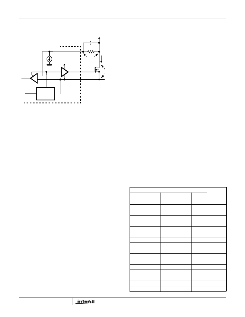
Resistors (R
OCSET1
and R
OCSET2
) program the over-
current trip levels for each PWM converter. As shown in
Figure 9, the internal 200
μ
A current sink develops a voltage
across R
OCSET
(V
SET
) that is referenced to V
IN
. The DRIVE
signal enables the over-current comparator (OVER-
CURRENT1 or OVER-CURRENT2). When the voltage
across the upper MOSFET (V
DS
) exceeds V
SET
, the over-
current comparator trips to set the over-current latch. Both
V
SET
and V
DS
are referenced to V
IN
and a small capacitor
across R
OCSET
helps V
OCSET
track the variations of V
IN
due
to MOSFET switching. The over-current function will trip at a
peak inductor current (I
PEAK)
determined by:
)
The OC trip point varies with MOSFET’s temperature. To avoid
over-current tripping in the normal operating load range,
determine the R
OCSET
resistor from the equation above with:
1. The maximum r
DS(ON)
at the highest junction temperature.
2. The minimum I
OCSET
from the specification table.
3. Determine I
PEAK
for I
PEAK
> I
OUT(MAX)
+ (
I)/2,
where
I is the output inductor ripple current.
For an equation for the output inductor ripple current see the
section under component guidelines titled ‘Output Inductor
Selection’.
OUT1 Voltage Program
The output voltage of the PWM1 converter is programmed to
discrete levels between 1.3V
DC
and 3.5V
DC
. This output is
designed to supply the microprocessor core voltage. The
voltage identification (VID) pins program an internal voltage
reference (DACOUT) through a TTL-compatible 5-bit digital-to-
analog converter. The level of DACOUT also sets the PGOOD
and OVP thresholds. Table 1 specifies the DACOUT voltage for
the different combinations of connections on the VID pins. The
VID pins can be left open for a logic 1 input, because they are
internally pulled up to +5V by a 10
μ
A current source. Changing
the VID inputs during operation is not recommended. The
sudden change in the resulting reference voltage could toggle
the PGOOD signal and exercise the over-voltage protection.
The ‘11111’ VID pin combination resulting in an INHIBIT
disables the IC and the open-collector at the PGOOD pin.
Application Guidelines
Soft-Start Interval
Initially, the soft-start function clamps the error amplifiers’
output of the PWM converters. After the output voltage
increases to approximately 80% of the set value, the
reference input of the error amplifier is clamped to a voltage
proportional to the SS pin voltage. The resulting output
voltage sequence is shown in Figure 6.
The soft-start function controls the output voltage rate of rise
to limit the current surge at start-up. The soft-start interval is
programmed by the soft-start capacitor, C
SS
. Programming
a faster soft-start interval increases the peak surge current.
The peak surge current occurs during the initial output
voltage rise to 80% of the set value.
Shutdown
Neither PWM output switches until the soft-start voltage
(V
SS
) exceeds the oscillator’s valley voltage. Additionally,
the reference on each linear’s amplifier is clamped to the
soft-start voltage. Holding the SS pin low (with an open drain
or collector signal) turns off all four regulators.
The ‘11111’ VID code resulting in an INHIBIT as shown in
Table 1 also shuts down the IC.
UGATE
OCSET
PHASE
OVER-
CURRENT2
+
-
GATE
CONTROL
VCC
OC2
200
μ
A
V
DS
I
D
V
SET
R
OCSET
V
IN
= +5V
OVER-CURRENT TRIP: V
DS
> V
SET
(I
D
r
DS(ON)
> I
OCSET
R
OCSET
)
I
OCSET
+
+
FIGURE 9. OVER-CURRENT DETECTION
PWM
V
PHASE
= V
IN
- V
DS
V
OCSET
= V
IN
- V
SET
DRIVE
HIP6019B
IPEAK =
×
IOCSrDS ROCSET
TABLE 1.
PIN NAME
NOMINAL
OUT1
VOLTAGE
DACOUT
VID4
VID3
VID2
VID1
VID0
0
1
1
1
1
1.30
0
1
1
1
0
1.35
0
1
1
0
1
1.40
0
1
1
0
0
1.45
0
1
0
1
1
1.50
0
1
0
1
0
1.55
0
1
0
0
1
1.60
0
1
0
0
0
1.65
0
0
1
1
1
1.70
0
0
1
1
0
1.75
0
0
1
0
1
1.80
0
0
1
0
0
1.85
0
0
0
1
1
1.90
0
0
0
1
0
1.95
0
0
0
0
1
2.00
0
0
0
0
0
2.05
HIP6019B
相关PDF资料 |
PDF描述 |
|---|---|
| HIP6028EVAL1 | Advanced PWM and Dual Linear Power Control with Integrated ACPI Support Interface |
| HIP6028 | Advanced PWM and Dual Linear Power Control with Integrated ACPI Support Interface |
| HIP6028CB | Advanced PWM and Dual Linear Power Control with Integrated ACPI Support Interface |
| HIP6303CB-T | Microprocessor CORE Voltage Regulator Multi-Phase Buck PWM Controller |
| HIP6303 | Microprocessor CORE Voltage Regulator Multi-Phase Buck PWM Controller(微处理器核心电压稳压多相冲跳脉宽调制控制器) |
相关代理商/技术参数 |
参数描述 |
|---|---|
| HIP6019B_05 | 制造商:INTERSIL 制造商全称:Intersil Corporation 功能描述:Advanced Dual PWM and Dual Linear Power Control |
| HIP6019BBCB WAF | 制造商:Harris Corporation 功能描述: |
| HIP6019BCB | 功能描述:IC REG QD BCK/LINEAR 28-SOIC RoHS:否 类别:集成电路 (IC) >> PMIC - 稳压器 - 线性 + 切换式 系列:- 标准包装:2,500 系列:- 拓扑:降压(降压)同步(3),线性(LDO)(2) 功能:任何功能 输出数:5 频率 - 开关:300kHz 电压/电流 - 输出 1:控制器 电压/电流 - 输出 2:控制器 电压/电流 - 输出 3:控制器 带 LED 驱动器:无 带监控器:无 带序列发生器:是 电源电压:5.6 V ~ 24 V 工作温度:-40°C ~ 85°C 安装类型:* 封装/外壳:* 供应商设备封装:* 包装:* |
| HIP6019BCB-T | 功能描述:IC REG QD BCK/LINEAR 28-SOIC RoHS:否 类别:集成电路 (IC) >> PMIC - 稳压器 - 线性 + 切换式 系列:- 标准包装:2,500 系列:- 拓扑:降压(降压)同步(3),线性(LDO)(2) 功能:任何功能 输出数:5 频率 - 开关:300kHz 电压/电流 - 输出 1:控制器 电压/电流 - 输出 2:控制器 电压/电流 - 输出 3:控制器 带 LED 驱动器:无 带监控器:无 带序列发生器:是 电源电压:5.6 V ~ 24 V 工作温度:-40°C ~ 85°C 安装类型:* 封装/外壳:* 供应商设备封装:* 包装:* |
| HIP6019BCBZ | 功能描述:电压模式 PWM 控制器 ADV DL 3PWM & DL LINER PWR CONTROL RoHS:否 制造商:Texas Instruments 输出端数量:1 拓扑结构:Buck 输出电压:34 V 输出电流: 开关频率: 工作电源电压:4.5 V to 5.5 V 电源电流:600 uA 最大工作温度:+ 125 C 最小工作温度:- 40 C 封装 / 箱体:WSON-8 封装:Reel |
发布紧急采购,3分钟左右您将得到回复。