- 您现在的位置:买卖IC网 > PDF目录385382 > HIP6301VCBZ (INTERSIL CORP) Microprocessor CORE Voltage Regulator Multi-Phase Buck PWM Controller PDF资料下载
参数资料
| 型号: | HIP6301VCBZ |
| 厂商: | INTERSIL CORP |
| 元件分类: | 稳压器 |
| 英文描述: | Microprocessor CORE Voltage Regulator Multi-Phase Buck PWM Controller |
| 中文描述: | SWITCHING CONTROLLER, 1500 kHz SWITCHING FREQ-MAX, PDSO20 |
| 封装: | LEAD FREE, PLASTIC, MS-013AC, SOIC-20 |
| 文件页数: | 15/20页 |
| 文件大小: | 518K |
| 代理商: | HIP6301VCBZ |
15
FN9034.2
December 27, 2004
the sampled current (I
SAMPLE
) can be related to the load
current (I
LT
) by:
I
Where: I
LT
= total load current
n = the number of channels
Example: Using the previously given conditions, and
For I
LT
= 100A,
n = 4
Then I
SAMPLE
= 25.49A
As discussed previously, the voltage drop across each Q2
transistor at the point in time when current is sampled is
r
DSON
(Q2) x
I
SAMPLE
. The voltage at Q2’s drain, the
PHASE node, is applied through the R
ISEN
resistor to the
HIP6301V ISEN pin. This pin is held at virtual ground, so the
current into ISEN is:
I
------------------------------------------------------------------
=
Example: From the previous conditions,
where I
LT
I
SAMPLE
r
DS(ON)
(Q2)
Then: R
ISEN
I
CURRENT TRIP
Short circuit I
LT
= 100A,
= 25.49A,
= 4m
= 2.04K and
= 165%
= 165A.
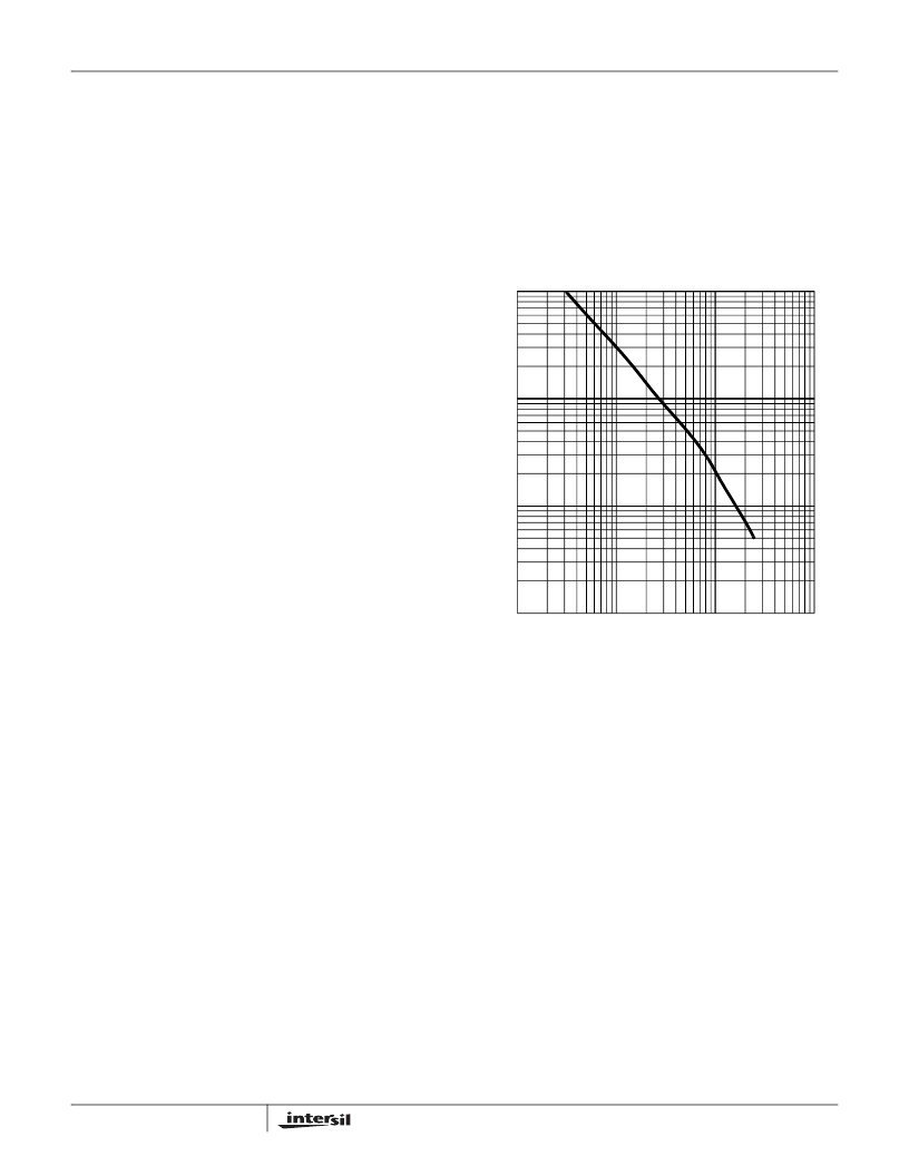
Channel Frequency Oscillator
The channel oscillator frequency is set by placing a resistor,
R
T
, to ground from the FS/DIS pin. Figure 12 is a curve
showing the relationship between frequency, F
SW,
and
resistor R
T
. To avoid pickup by the FS/DIS pin, it is important
to place this resistor next to the pin.
Layout Considerations
MOSFETs switch very fast and efficiently. The speed with
which the current transitions from one device to another
causes voltage spikes across the interconnecting
impedances and parasitic circuit elements. These voltage
spikes can degrade efficiency, radiate noise into the circuit
and lead to device overvoltage stress. Careful component
layout and printed circuit design minimizes the voltage
spikes in the converter. Consider, as an example, the turnoff
transition of the upper PWM MOSFET. Prior to turnoff, the
upper MOSFET was carrying channel current. During the
turnoff, current stops flowing in the upper MOSFET and is
picked up by the lower MOSFET. Any inductance in the
switched current path generates a large voltage spike during
the switching interval. Careful component selection, tight
layout of the critical components, and short, wide circuit
traces minimize the magnitude of voltage spikes. Contact
Intersil for evaluation board drawings of the component
placement and printed circuit board.
There are two sets of critical components in a DC-DC
converter using a HIP6301V or HIP6302V controller and a
HIP6601 family gate driver. The power components are the
most critical because they switch large amounts of energy.
Next are small signal components that connect to sensitive
nodes or supply critical bypassing current and signal coupling.
The power components should be placed first. Locate the
input capacitors close to the power switches. Minimize the
length of the connections between the input capacitors, C
IN
,
and the power switches. Locate the output inductors and
output capacitors between the MOSFETs and the load.
Locate the gate driver close to the MOSFETs.
The critical small components include the bypass capacitors
for VCC and PVCC on the gate driver ICs. Locate the bypass
capacitor, C
BP
, for the controller close to the device. It is
especially important to locate the resistors associated with the
input to the amplifiers close to their respective pins, since they
represent the input to feedback amplifiers. Resistor R
T
, that
sets the oscillator frequency should also be located next to the
associated pin. It is especially important to place the R
SEN
resistor(s) at the respective ISEN terminals.
A multi-layer printed circuit board is recommended. Figure 13
shows the connections of the critical components for one output
channel of the converter. Note that capacitors C
IN
and C
OUT
could each represent numerous physical capacitors. Dedicate
one solid layer, usually the middle layer of the PC board, for a
ground plane and make all critical component ground connections
I
SAMPLE
-------
-----------------------------------------------------------------------------------
V
IN
(
)
V
CORE
SW
3V
2
–
+
IN
=
I
SENSE
(
)
r
ISEN
Q2
(
)
R
ISEN
I
------------------------------------------------------------------
(
)
r
Q2
(
)
=
50
100
10
20
CHANNEL OSCILLATOR FREQUENCY, FSW (kHz)
200
500 1,000
5,000 10,000
2,000
1
2
5
10
20
50
100
200
500
1,000
R
FIGURE 12. RESISTANCE R
T
vs FREQUENCY
HIP6301V, HIP6302V
相关PDF资料 |
PDF描述 |
|---|---|
| HIP6311A | 150000 SYSTEM GATE 2.5 VOLT FPGA - NOT RECOMMENDED for NEW DESIGN |
| HIP6311ACB | Microprocessor CORE Voltage Regulator Multi-Phase Buck PWM Controller |
| HIP6311ACBZ | Microprocessor CORE Voltage Regulator Multi-Phase Buck PWM Controller |
| HIP6311ACBZ-T | Microprocessor CORE Voltage Regulator Multi-Phase Buck PWM Controller |
| HIP6311ACBZA | XCV150-5BGG352I - NOT RECOMMENDED for NEW DESIGN |
相关代理商/技术参数 |
参数描述 |
|---|---|
| HIP6301VCBZA | 制造商:INTERSIL 制造商全称:Intersil Corporation 功能描述:Microprocessor CORE Voltage Regulator Multi-Phase Buck PWM Controller |
| HIP6301VCBZA-T | 制造商:INTERSIL 制造商全称:Intersil Corporation 功能描述:Microprocessor CORE Voltage Regulator Multi-Phase Buck PWM Controller |
| HIP6301VCBZ-T | 功能描述:电流型 PWM 控制器 MULTI-PHS CNTRLR VID ON THE FLYINTEL VID RoHS:否 制造商:Texas Instruments 开关频率:27 KHz 上升时间: 下降时间: 工作电源电压:6 V to 15 V 工作电源电流:1.5 mA 输出端数量:1 最大工作温度:+ 105 C 安装风格:SMD/SMT 封装 / 箱体:TSSOP-14 |
| HIP6302 | 制造商:INTERSIL 制造商全称:Intersil Corporation 功能描述:Microprocessor CORE Voltage Regulator Multi-Phase Buck PWM Controller |
| HIP6302_04 | 制造商:INTERSIL 制造商全称:Intersil Corporation 功能描述:Microprocessor CORE Voltage Regulator Multi-Phase Buck PWM Controller |
发布紧急采购,3分钟左右您将得到回复。