- 您现在的位置:买卖IC网 > PDF目录371822 > HIP6604BCR (INTERSIL CORP) FPGA 2000000 SYSTEM GATE 1.8 VOLT - NOT RECOMMENDED for NEW DESIGN PDF资料下载
参数资料
| 型号: | HIP6604BCR |
| 厂商: | INTERSIL CORP |
| 元件分类: | 功率晶体管 |
| 英文描述: | FPGA 2000000 SYSTEM GATE 1.8 VOLT - NOT RECOMMENDED for NEW DESIGN |
| 中文描述: | 0.73 A HALF BRDG BASED MOSFET DRIVER, PQCC16 |
| 封装: | 4 X 4 MM, PLASTIC, MO-220VGGC, QFN-16 |
| 文件页数: | 7/11页 |
| 文件大小: | 346K |
| 代理商: | HIP6604BCR |
7
FN9072.7
July 20, 2005
be performed to ensure safe operation at the desired
frequency for the selected MOSFETs. The power dissipated
by the driver is approximated as:
where f
sw
is the switching frequency of the PWM signal. V
U
and V
L
represent the upper and lower gate rail voltage. Q
U
and Q
L
is the upper and lower gate charge determined by
MOSFET selection and any external capacitance added to
the gate pins. The I
DDQ
V
CC
product is the quiescent power
of the driver and is typically 30mW.
The power dissipation approximation is a result of power
transferred to and from the upper and lower gates. But, the
internal bootstrap device also dissipates power on-chip
during the refresh cycle. Expressing this power in terms of
the upper MOSFET total gate charge is explained below.
The bootstrap device conducts when the lower MOSFET or
its body diode conducts and pulls the PHASE node toward
GND. While the bootstrap device conducts, a current path is
formed that refreshes the bootstrap capacitor. Since the
upper gate is driving a MOSFET, the charge removed from
the bootstrap capacitor is equivalent to the total gate charge
of the MOSFET. Therefore, the refresh power required by
the bootstrap capacitor is equivalent to the power used to
charge the gate capacitance of the MOSFET.
where Q
LOSS
is the total charge removed from the bootstrap
capacitor and provided to the upper gate load.
The 1.05 factor is a correction factor derived from the
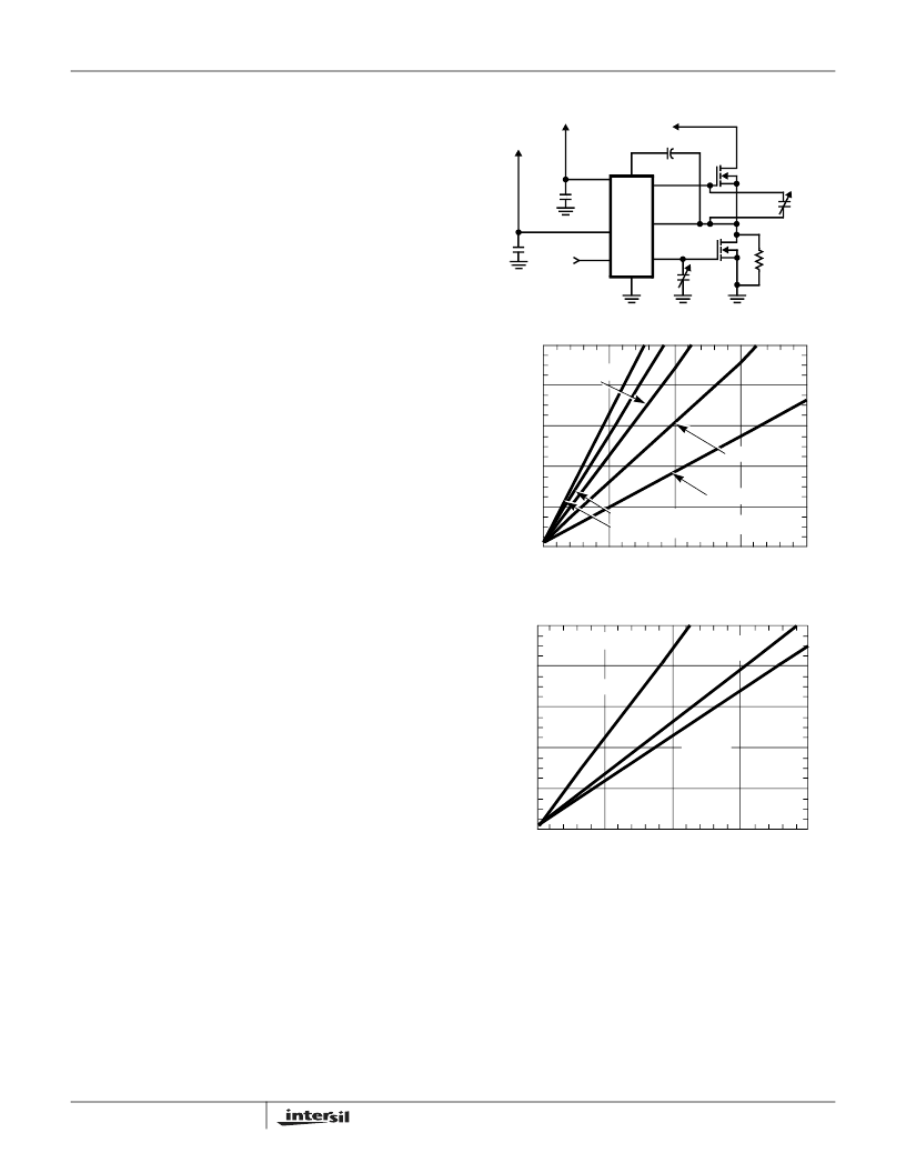
following characterization. The base circuit for characterizing
the drivers for different loading profiles and frequencies is
provided. C
U
and C
L
are the upper and lower gate load
capacitors. Decoupling capacitors [0.15
μ
F] are added to the
PVCC and VCC pins. The bootstrap capacitor value is
0.01
μ
F.
In Figure 1, C
U
and C
L
values are the same and frequency
is varied from 50kHz to 2MHz. PVCC and VCC are tied
together to a +12V supply. Curves do exceed the 800mW
cutoff, but continuous operation above this point is not
recommended.
Figure 2 shows the dissipation in the driver with 3nF loading
on both gates and each individually. Note the higher upper
gate power dissipation which is due to the bootstrap device
refresh cycle. Again PVCC and VCC are tied together and to
a +12V supply.
Test Circuit
The impact of loading on power dissipation is shown in
Figure 3. Frequency is held constant while the gate capacitors
are varied from 1nF to 5nF. VCC and PVCC are tied together
and to a +12V supply. Figures 4, 5 and 6 show the same
characterization for the HIP6603B with a +5V supply on PVCC
and VCC tied to a +12V supply.
Since both upper and lower gate capacitance can vary,
Figure 8 shows dissipation curves versus lower gate
capacitance with upper gate capacitance held constant at three
different values. These curves apply only to the HIP6601B due
to power supply configuration.
P
1.05f
sw
3
2
--
V
U
Q
U
V
L
Q
L
+
I
DDQ
VCC
+
=
P
REFRESH
1
2
--
f
SW
Q
LOSS
V
PVCC
1
2
--
f
SW
Q
U
V
U
=
=
BOOT
UGATE
PHASE
LGATE
PWM
PVCC
GND
VCC
0.15
μ
F
0.15
μ
F
100k
2N7002
2N7002
C
L
0.01
μ
F
C
U
+5V OR +12V
+12V
H
+5V OR +12V
FIGURE 1. POWER DISSIPATION vs FREQUENCY
1000
800
600
400
200
0
500
1000
1500
2000
P
FREQUENCY (kHz)
C
U
= C
L
= 3nF
VCC = PVCC = 12V
C
U
= C
L
= 1nF
C
U
= C
L
= 2nF
C
U
= C
L
= 4nF
C
U
= C
L
= 5nF
FIGURE 2. 3nF LOADING PROFILE
1000
800
600
400
200
0
500
1000
1500
2000
P
FREQUENCY (kHz)
C
U
= C
L
= 3nF
VCC = PVCC = 12V
C
U
= 3nF
C
L
= 0nF
C
U
= 0nF
C
L
= 3nF
HIP6601B, HIP6603B, HIP6604B
相关PDF资料 |
PDF描述 |
|---|---|
| HIP6603B | Synchronous Rectified Buck MOSFET Drivers |
| HIP6603BCB | FPGA 1600000 SYSTEM GATE 1.8 VOLT - NOT RECOMMENDED for NEW DESIGN |
| HIP6603BCB-T | Synchronous Rectified Buck MOSFET Drivers |
| HIP6601BECB | Synchronous Rectified Buck MOSFET Drivers |
| HIP6603BECB | Synchronous Rectified Buck MOSFET Drivers |
相关代理商/技术参数 |
参数描述 |
|---|---|
| HIP6604BCR-T | 功能描述:IC DRIVER MOSF SYNC BUCK 16-QFN RoHS:否 类别:集成电路 (IC) >> PMIC - MOSFET,电桥驱动器 - 外部开关 系列:- 标准包装:50 系列:- 配置:低端 输入类型:非反相 延迟时间:40ns 电流 - 峰:9A 配置数:1 输出数:1 高端电压 - 最大(自引导启动):- 电源电压:4.5 V ~ 35 V 工作温度:-40°C ~ 125°C 安装类型:表面贴装 封装/外壳:TO-263-6,D²Pak(5 引线+接片),TO-263BA 供应商设备封装:TO-263 包装:管件 |
| HIP6604BCRZ | 功能描述:功率驱动器IC SYNCH-RECTIFIED BUCK MSFT DRVR 16LD RoHS:否 制造商:Micrel 产品:MOSFET Gate Drivers 类型:Low Cost High or Low Side MOSFET Driver 上升时间: 下降时间: 电源电压-最大:30 V 电源电压-最小:2.75 V 电源电流: 最大功率耗散: 最大工作温度:+ 85 C 安装风格:SMD/SMT 封装 / 箱体:SOIC-8 封装:Tube |
| HIP6604BCRZ-T | 功能描述:功率驱动器IC SYNCH-RECTIFIED BUCK MSFT DRVR 16LD RoHS:否 制造商:Micrel 产品:MOSFET Gate Drivers 类型:Low Cost High or Low Side MOSFET Driver 上升时间: 下降时间: 电源电压-最大:30 V 电源电压-最小:2.75 V 电源电流: 最大功率耗散: 最大工作温度:+ 85 C 安装风格:SMD/SMT 封装 / 箱体:SOIC-8 封装:Tube |
| HIP6604CR | 制造商:INTERSIL 制造商全称:Intersil Corporation 功能描述:Synchronous Rectified Buck MOSFET Drivers |
| HIP6604CR-T | 制造商:INTERSIL 制造商全称:Intersil Corporation 功能描述:Synchronous Rectified Buck MOSFET Drivers |
发布紧急采购,3分钟左右您将得到回复。