- 您现在的位置:买卖IC网 > PDF目录384465 > HY29LV320TT-90I (HYNIX SEMICONDUCTOR INC) 32 Mbit (2M x 16) Low Voltage Flash Memory PDF资料下载
参数资料
| 型号: | HY29LV320TT-90I |
| 厂商: | HYNIX SEMICONDUCTOR INC |
| 元件分类: | DRAM |
| 英文描述: | 32 Mbit (2M x 16) Low Voltage Flash Memory |
| 中文描述: | 2M X 16 FLASH 3V PROM, 90 ns, PDSO48 |
| 封装: | TSOP-48 |
| 文件页数: | 11/44页 |
| 文件大小: | 323K |
| 代理商: | HY29LV320TT-90I |
第1页第2页第3页第4页第5页第6页第7页第8页第9页第10页当前第11页第12页第13页第14页第15页第16页第17页第18页第19页第20页第21页第22页第23页第24页第25页第26页第27页第28页第29页第30页第31页第32页第33页第34页第35页第36页第37页第38页第39页第40页第41页第42页第43页第44页
11
r1.3/May 02
HY29LV320
WE#
ADR
CE#
OE#
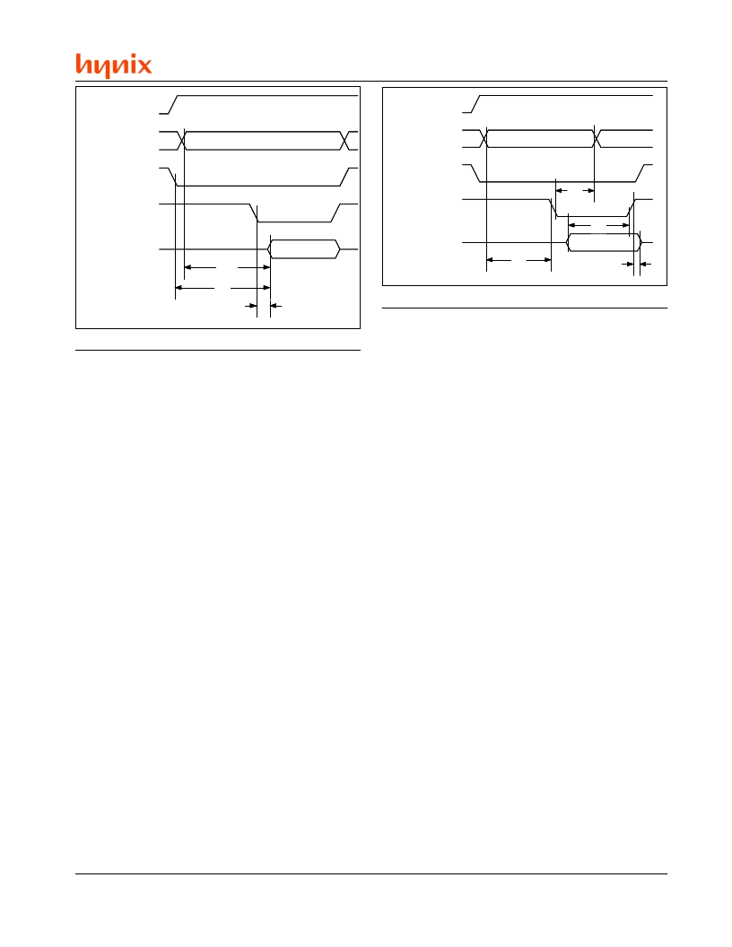
Figure 1. Read Operation
Write Operation
Figure 2. Write Operation
OE#
ADR
CE#
WE#
DATA
OUT
t
ACC
t
CE
t
OE
DATA
IN
t
AS
t
AH
t
DH
t
DS
Certain operations, including programming data
and erasing sectors of memory, require the host
to write a command or command sequence to the
HY29LV320. Writes to the device are performed
by placing the word address on the device
’
s ad-
dress inputs while the data to be written is input
on DQ[15:0]. The host system must drive the CE#
and WE# pins Low and drive OE# High for a valid
write operation to take place. All addresses are
latched on the falling edge of WE# or CE#, which-
ever happens later. All data is latched on the ris-
ing edge of WE# or CE#, whichever happens first.
See Figure 2.
.The
“
Device Commands
”
section of this specifi-
cation provides details on the specific device com-
mands implemented in the HY29LV320.
Accelerated Program Operation
This device offers accelerated program operations
through the
“
Accelerate
”
function provided by the
WP#/ACC pin. This function is intended primarily
for faster programming throughput at the factory.
If V
HH
is applied to the WP#/ACC input, the device
enters the Unlock Bypass mode, temporarily
unprotects any protected sectors, and uses the
higher voltage on the pin to reduce the time re-
quired for program operations. The system would
then use the two-cycle program command se-
quence as required by the Unlock Bypass mode.
Removing V
HH
from the pin returns the device to
normal operation.
Note:
WP# sector protection cannot be used while WP#/
ACC = V
. Thus, all sectors are unprotected and can
be erased and programmed while in Accelerated Pro-
gramming mode.
Note:
The Accelerate function does not affect the time
required for Erase operations.
See the description of the WP#/ACC pin in the
Pin Descriptions table for additional information
on this function.
Write Protect Function
The Write Protect function provides a hardware
method of protecting the boot sectors without us-
ing V
ID
. This function is a second function pro-
vided by the WP#/ACC pin.
Placing this pin at V
IL
disables program and erase
operations in the bottom or top 32K words of the
array (the boot sectors). The affected sectors are
as follows (see Tables 1 and 2):
HY29LV320B: S0
–
S3
HY29LV320T: S63
–
S66
If the pin is placed at V
IH
, the protection state of
those sectors reverts to whether they were last
set to be protected or unprotected using the
method described in the Sector Group Protection
and Unprotection sections.
Note:
Sectors protected by WP#/ACC = V
remain pro-
tected during Temporary Sector Unprotect and cannot
be erased or programmed. Also see note under Accel-
erate Program Operation above.
Standby Operation
When the system is not reading or writing to the
device, it can place the device in the Standby
相关PDF资料 |
PDF描述 |
|---|---|
| HY29LV320BF-70 | 32 Mbit (2M x 16) Low Voltage Flash Memory |
| HY29LV320BT-12 | SWITCH TOGGLE SPST SCREW 15A |
| HY29LV320TF-12 | 122 x 32 pixel format, LED Backlight available |
| HY29LV320TF-12I | 122 x 32 pixel format, LED Backlight available |
| HY29LV320TT-12 | 150 x 32 pixel format, LED Backlight available |
相关代理商/技术参数 |
参数描述 |
|---|---|
| HY29LV400 | 制造商:未知厂家 制造商全称:未知厂家 功能描述:4M(X8/X16)|3.0V|55|NOR FLASH - 4M |
| HY29LV400BF55 | 制造商:HYNIX 制造商全称:Hynix Semiconductor 功能描述:4 Mbit (512K x 8/256K x 16) Low Voltage Flash Memory |
| HY29LV400BF55I | 制造商:HYNIX 制造商全称:Hynix Semiconductor 功能描述:4 Mbit (512K x 8/256K x 16) Low Voltage Flash Memory |
| HY29LV400BF70 | 制造商:HYNIX 制造商全称:Hynix Semiconductor 功能描述:4 Mbit (512K x 8/256K x 16) Low Voltage Flash Memory |
| HY29LV400BF70I | 制造商:HYNIX 制造商全称:Hynix Semiconductor 功能描述:4 Mbit (512K x 8/256K x 16) Low Voltage Flash Memory |
发布紧急采购,3分钟左右您将得到回复。