- 您现在的位置:买卖IC网 > PDF目录67683 > IBM25PPC750CXEJQ5012T 32-BIT, 500 MHz, RISC PROCESSOR, PBGA256 PDF资料下载
参数资料
| 型号: | IBM25PPC750CXEJQ5012T |
| 元件分类: | 微控制器/微处理器 |
| 英文描述: | 32-BIT, 500 MHz, RISC PROCESSOR, PBGA256 |
| 封装: | 27 X 27 MM, LEAD FREE, PLASTIC, BGA-256 |
| 文件页数: | 14/44页 |
| 文件大小: | 416K |
| 代理商: | IBM25PPC750CXEJQ5012T |
第1页第2页第3页第4页第5页第6页第7页第8页第9页第10页第11页第12页第13页当前第14页第15页第16页第17页第18页第19页第20页第21页第22页第23页第24页第25页第26页第27页第28页第29页第30页第31页第32页第33页第34页第35页第36页第37页第38页第39页第40页第41页第42页第43页第44页
Data Sheet
Preliminary
PowerPC 750CXe RISC Microprocessor
750cxe_DD3.1_Dev_3_gen_mkt.fm.1.5
April 8, 2004
Electrical and Thermal Characteristics
Page 13 of 36
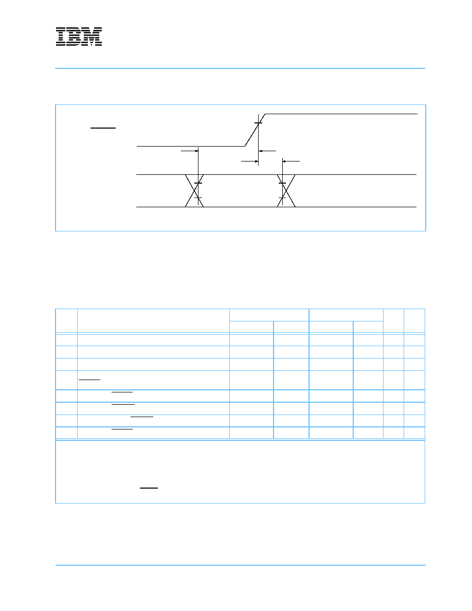
Figure 4-4 provides the mode select input timing diagram for the PowerPC 750CXe.
4.5 60x Bus Output AC Specifications
Table 4-8 provides the 60x bus output AC timing specifications for the PowerPC 750CXe as defined in
Figure 4-4. Mode Select Input Timing Diagram
Table 4-8. 60x Bus Output AC Timing Specifications1,4,6 See Table 4-2 on page 7 for operating conditions.
Num
Characteristic
1.8V Mode
2.5 V Mode
Unit
Notes
Min.
Max.
Min.
Max.
12
SYSCLK to Output Driven (Output Enable Time)
0.3
ns
13
SYSCLK to Output Valid
–
2.20
–
2.20
ns
14
SYSCLK to Output Invalid (Output Hold)
0.500
0.400
ns
2
15
SYSCLK to Output High Impedance (all signals except
ARTRY)
–2.5
–
2.5
ns
16
SYSCLK to ARTRY high impedance before precharge
–
3.0
–
3.0
ns
17
SYSCLK to ARTRY precharge enable
0.2t
SYSCLK+1.0
0.2t
SYSCLK+1.0
ns
2, 3, 5
18
Maximum delay to ARTRY precharge
1
t
SYSCLK
3, 5
19
SYSCLK to ARTRY high impedance after precharge
2
t
SYSCLK
3, 5
Notes:
1. All output specifications are measured from the midpoint voltage (0.8V) of the rising edge of SYSCLK to the midpoint voltage of the signal in question
defined in figure 4-5. Both input and output timings are measured at the pin. Timings are determined by design.
2. This minimum parameter assumes CL = 0pF.
3. t
SYSCLK is the period of the external bus clock (SYSCLK) in nanoseconds (ns). The numbers given in the table must be multiplied by the period of
SYSCLK to compute the actual time duration of the parameter in question.
4. Output signal transitions are defined in figure 4-5.
5. Nominal precharge width for ARTRY is 1.0 t
SYSCLK.
6. Guaranteed by design and characterization, and not tested.
VIH
V
IH = +1.24 V
MODE PINS
10c
11b
HRESET
10c
11b
相关PDF资料 |
PDF描述 |
|---|---|
| IBM25PPC750CXEJQ4012T | 32-BIT, 466 MHz, RISC PROCESSOR, PBGA256 |
| IBM25PPC750CXEJQ2013T | 32-BIT, 400 MHz, RISC PROCESSOR, PBGA256 |
| IBM25PPC750CXEJP5513T | 32-BIT, 533 MHz, RISC PROCESSOR, PBGA256 |
| IBM25PPC750CXEJP2013T | 32-BIT, 400 MHz, RISC PROCESSOR, PBGA256 |
| IBM25PPC750CXEJP5512T | 32-BIT, 533 MHz, RISC PROCESSOR, PBGA256 |
相关代理商/技术参数 |
参数描述 |
|---|---|
| IBM25PPC750FL-GR0123V | 制造商:IBM 功能描述:MPU 750XX RISC 32BIT - Trays |
| IBM25PPC750FL-GR0124V | 制造商:IBM 功能描述:MPU 750XX RISC 32BIT - Trays |
| IBM25PPC750FL-GR0133T | 制造商:IBM 功能描述:IBMIBM25PPC750FL-GR0133T CSOI9SG LOGIC P |
| IBM25PPC750FL-GR0133V | 制造商:IBM 功能描述:MPU 750XX RISC 32BIT - Trays |
| IBM25PPC750FL-GR1024T | 制造商:IBM 功能描述: |
发布紧急采购,3分钟左右您将得到回复。