- 您现在的位置:买卖IC网 > PDF目录261240 > IBM25PPC750FX-DB2513T 32-BIT, 800 MHz, RISC PROCESSOR, CBGA292 PDF资料下载
参数资料
| 型号: | IBM25PPC750FX-DB2513T |
| 元件分类: | 微控制器/微处理器 |
| 英文描述: | 32-BIT, 800 MHz, RISC PROCESSOR, CBGA292 |
| 封装: | 21 X 21 MM, 1 MM PITCH, CERAMIC, BGA-292 |
| 文件页数: | 50/62页 |
| 文件大小: | 452K |
| 代理商: | IBM25PPC750FX-DB2513T |
第1页第2页第3页第4页第5页第6页第7页第8页第9页第10页第11页第12页第13页第14页第15页第16页第17页第18页第19页第20页第21页第22页第23页第24页第25页第26页第27页第28页第29页第30页第31页第32页第33页第34页第35页第36页第37页第38页第39页第40页第41页第42页第43页第44页第45页第46页第47页第48页第49页当前第50页第51页第52页第53页第54页第55页第56页第57页第58页第59页第60页第61页第62页
DD 2.X
PowerPC 750FX RISC Microprocessor
Preliminary
5. System Design Information
Page 52 of 63
Body_750FX_DS_DD2.X.fm.2.0
June 9, 2003
5.8.2 Internal Package Conduction
For the exposed-die packaging technology, shown in Table 3-3 Package Thermal Characteristics1 on
page 10, the intrinsic conduction thermal resistance paths are as follows.
Die junction-to-case thermal resistance (Primary thermal path)
Die junction-to-lead thermal resistance (Not normally a signicant thermal path)
Die junction-to-ambient thermal resistance (Largely dependent on customer-supplied heatsink)
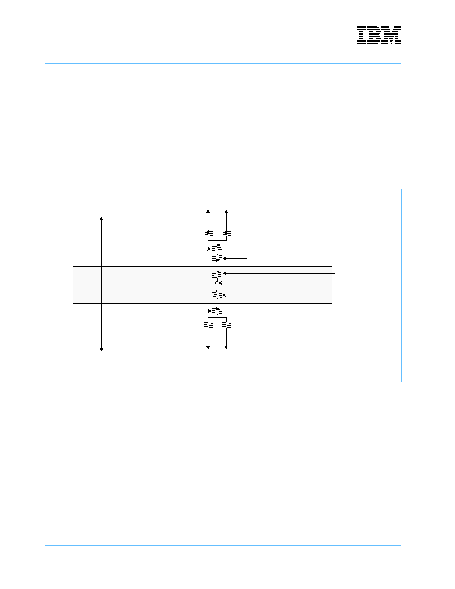
Figure 5-9 depicts the primary heat transfer path for a package with an attached heat sink mounted to a
printed-circuit board.
Heat generated on the active side (ball) of the chip is conducted through the silicon, then through the heat
sink attach material (or thermal interface material), and finally to the heat sink; where it is removed by forced-
air convection. Since the silicon thermal resistance is quite small, for a first-order analysis, the temperature
drop in the silicon may be neglected. Thus, the heat sink attach material and the heat sink conduc-
tion/convective thermal resistances are the dominant terms.
The heat flow path from the die, through the chip-to-substrate balls, through the substrate, through the
substrate-to-board balls, and through the board to ambient is usually too high of a resistance to offer much
cooling. In addition, various factors make the heat flow through this path very difficult to accurately determine.
Designers must not depend on cooling the 750FX using this means unless thermal modeling has been confi-
dently completed.
Figure 5-9. C4 Package with Heat Sink Mounted to a Printed-Circuit Board
External Resistance
Internal
(Note the internal versus external package resistance.)
Radiation
Convection
Radiation
Convection
Heat Sink
Die/Package
Printed-Circuit Board
Thermal Interface Material
Package/Leads
Chip Junction
Resistance
相关PDF资料 |
PDF描述 |
|---|---|
| ICS87950AY-T | 180 MHz, OTHER CLOCK GENERATOR, PQFP32 |
| ICS84329BM-01 | 700 MHz, OTHER CLOCK GENERATOR, PDSO28 |
| IBM25PPC750CXEJP5022T | 32-BIT, 500 MHz, RISC PROCESSOR, PBGA256 |
| IBM25PPC750GXEBB1033T | 32-BIT, 733 MHz, RISC PROCESSOR, CBGA292 |
| ICS525-01RILF | 140 MHz, OTHER CLOCK GENERATOR, PDSO28 |
相关代理商/技术参数 |
参数描述 |
|---|---|
| IBM25PPC750FX-FB1013T | 制造商:IBM 功能描述:32-BIT, 733 MHZ, RISC PROCESSOR, CBGA292 |
| IBM25PPC750FX-FB2513T | 制造商:IBM 功能描述:32-BIT, 800 MHz, RISC PROCESSOR, CBGA292 |
| IBM25PPC750FX-GB0122V | 制造商:IBM 功能描述:MPU 750XX RISC 32BIT - Trays |
| IBM25PPC750FX-GB0132T | 制造商:IC'S/TRANSISTORS/DIO 功能描述: 制造商:IC'S/TRANSISTORS/DIODES 功能描述: |
| IBM25PPC750FX-GB0132V | 制造商:IBM 功能描述:MPU 750XX RISC 32BIT - Trays |
发布紧急采购,3分钟左右您将得到回复。